
Datasheet


© 2009 Microchip Technology Inc. DS22005B-page 21
MCP73833/4
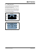
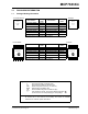
6.2 PCB Layout Issues
For optimum voltage regulation, place the battery pack
as close as possible to the device’s V
BAT
and V
SS
pins,
recommended to minimize voltage drops along the
high current-carrying PCB traces.
If the PCB layout is used as a heatsink, adding many
vias in the heatsink pad can help conduct more heat to
the backplane of the PCB, thus reducing the maximum
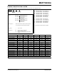
junction temperature. Figures 6-4 and 6-5 depict a
typical layout with PCB heatsinking.
FIGURE 6-4: Typical Layout (Top).
FIGURE 6-5: Typical Layout (Bottom).
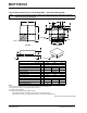
MCP73833
V
BAT
V
DD
V
SS
C
IN
C
OUT
THERM
PG
STAT1
STAT2
R
PROG
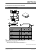
V
BAT
V
SS
V
DD