
User manual


Table Of Contents
- Introduction
- Document Layout
- Conventions Used in this Guide
- Recommended Reading
- The Microchip Web Site
- Customer Support
- Document Revision History
- Chapter 1. Product Overview
- 1.1 Introduction
- 1.2 MCP6XXX Amplifier Evaluation Board 4 Kit Contents
- 1.3 MCP6XXX Amplifier Evaluation Board 4 Description
- Chapter 2. Installation and Operation
- 2.1 Introduction
- 2.2 Required Tools
- 2.3 MCP6XXX Amplifier Evaluation Board 4 Set-up
- 2.4 MCP6XXX Amplifier Evaluation Board 4 Operation
- A.1 Introduction
- A.2 Board - Schematic
- A.3 Board - Top Silk and Metal Layers
- A.4 Board - Top Metal Layer
- A.5 Board - Bottom Metal Layer
- B.1 MCP6XXX Amplifier Evaluation Board 4 BOM
Installation and Operation
© 2007 Microchip Technology Inc. DS51681A-page 11
2.4 MCP6XXX AMPLIFIER EVALUATION BOARD 4 OPERATION
Items discussed in this section include:
• Building the Amplifier
• Testing the Amplifier
• Amplifier Modification: Using 8-Pin SOIC Op Amps
2.4.1 Building the Amplifier
This inverting integrator is described as follows:
• Power Supply V
DD
is 5.0V
• Load Capacitance C
L
is 56 pF
• Load Resistance R
L
is 1.6 kΩ
•R
1
= 8.06 kΩ, R
2
is open, R
3
= 8.06 kΩ, C
1
= 1 μF, R
ISO
= 0Ω
• Input Reference V
REF
= 0.5V
DD
• Integrator Control Strategy: Feedback Loop (JP1: Position 1, JP2: Position 1, JP3:
Position 1, JP4: Position 1)
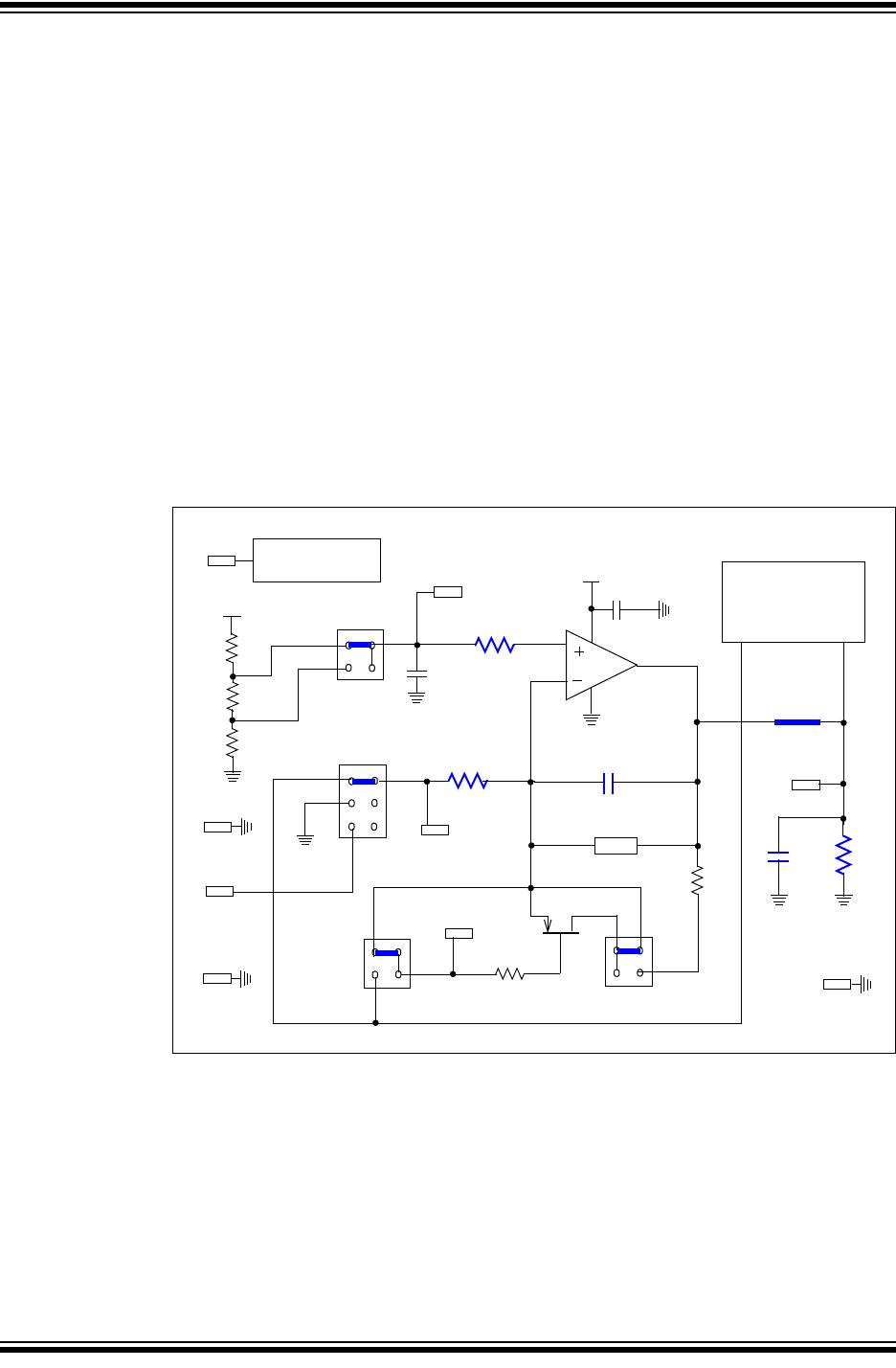
• The fully assembled inverting integrator is shown in Figure 2-6.
FIGURE 2-6: Inverting Integrator Example Supported by the MCP6XXX
Amplifier Evaluation Board 4.
*
VREF
C3
0.1 µF
RL
U1
VDD
0.1 µF
CU1
CL
2
3
1
2
1
2
1
C1
R2
R3
M1
R4
JP1
JP2
RV1
RV2
RV3
10k
8k
2k
100
100
R1
JP3
Non-Inverting
Comparator
Block
VDD
GND
VL
*
*
Power Supply
Block
Test Point
*
*
*
VIN
VSW
*
VINX
VDD
R5
*
GND
*
GND
*
2
1
JP4
RISO