
User manual


Table Of Contents
- Introduction
- Document Layout
- Conventions Used in this Guide
- Recommended Reading
- The Microchip Web Site
- Customer Support
- Document Revision History
- Chapter 1. Product Overview
- 1.1 Introduction
- 1.2 MCP6XXX Amplifier Evaluation Board 4 Kit Contents
- 1.3 MCP6XXX Amplifier Evaluation Board 4 Description
- Chapter 2. Installation and Operation
- 2.1 Introduction
- 2.2 Required Tools
- 2.3 MCP6XXX Amplifier Evaluation Board 4 Set-up
- 2.4 MCP6XXX Amplifier Evaluation Board 4 Operation
- A.1 Introduction
- A.2 Board - Schematic
- A.3 Board - Top Silk and Metal Layers
- A.4 Board - Top Metal Layer
- A.5 Board - Bottom Metal Layer
- B.1 MCP6XXX Amplifier Evaluation Board 4 BOM
MCP6XXX Amplifier Evaluation Board 4 User’s Guide
DS51681A-page 10 © 2007 Microchip Technology Inc.
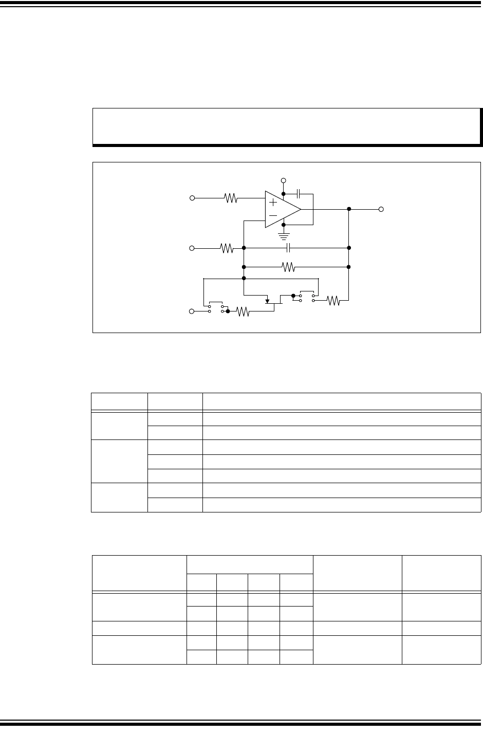
2.3.2 Inverting Integrator
• It integrates and inverts a voltage with an integrating frequency ω =1/R
1
C
1
(rad/s). Additional components control output clipping (wind-up) and initialization
of the integrating capacitor (C
1
). Refer to Figure 2-1.
• Figure 2-5 shows the circuit diagram for the inverting integrator block.
C
U1
= 0.1 uF, R
4
= R
5
= 100.0Ω, M
1
is N-MOSFET, R
3
= R
1
//R
2
FIGURE 2-5: Inverting Integrator Block.
Table 2-1 shows the jumper positions and the corresponding effects
TABLE 2-1: JUMPER POSITIONS AND EFFECTS
Table 2-2 shows the integrator control strategies
TABLE 2-2: INTEGRATOR CONTROL STRATEGY
Note 1: Adding R
2
to avoid the integrator output clipping at DC.
2: Adding R
3
to minimize the output error due to the input bias current
V
DD
C
U1
R
3
C
1
V
IN
R
1
R
2
M
1
V
R
V
OUT
R
4
V
CN
T
R5
U1
Inverting Integrator
100Ω
100Ω
JP4
JP3
# 1
# 2
# 1
# 2
Jumper Position Effect
JP
1
1 Set the Input Reference (V
REF
) to 0.5V
DD
2 Set the Input Reference (V
REF
)) to 0.1V
DD
JP
2
1 Drive Integrator with Comparator
2 Ground Integrator’s Resistor (contstant input current)
3 Drive Integrator with External Source
JP
3
, JP
4
1 Ground (de-activate) Integrator’s Reset Switch (M
1
)
2 Drive Integrator’s Reset Switch (M
1
) with Comparator
Integrator Control
Strategy
Jumper Positions
Integrator’s Input
Voltage
R2 (Integrator)
JP1 JP2 JP3 JP4
Feedback Loop
(1)
1 1 1 1 VCMP (internal) open
21 1 1
Reset Switch
(2)
2 2 2 2 GND (internal) open
Stand Alone 1 3 1 1 VINX >> R1
23 1 1
Note 1: The circuit shown uses a non-inverting comparator to close the feedback loop.
2: The reset switch (MOSFET) in the circuit is controlled by a non-inverting
comparator.