
User manual


Table Of Contents
- Introduction
- Document Layout
- Conventions Used in this Guide
- Recommended Reading
- The Microchip Web Site
- Customer Support
- Document Revision History
- Chapter 1. Product Overview
- 1.1 Introduction
- 1.2 MCP6XXX Amplifier Evaluation Board 4 Kit Contents
- 1.3 MCP6XXX Amplifier Evaluation Board 4 Description
- Chapter 2. Installation and Operation
- 2.1 Introduction
- 2.2 Required Tools
- 2.3 MCP6XXX Amplifier Evaluation Board 4 Set-up
- 2.4 MCP6XXX Amplifier Evaluation Board 4 Operation
- A.1 Introduction
- A.2 Board - Schematic
- A.3 Board - Top Silk and Metal Layers
- A.4 Board - Top Metal Layer
- A.5 Board - Bottom Metal Layer
- B.1 MCP6XXX Amplifier Evaluation Board 4 BOM
Installation and Operation
© 2007 Microchip Technology Inc. DS51681A-page 9
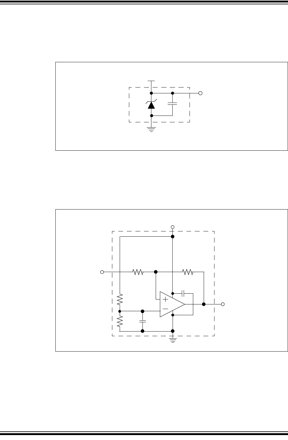
2.3.1 Top Level Amplifier Circuit Diagrams
2.3.1.1 POWER SUPPLY BLOCK
The power supply is protected by a zener diode and bypassed by a capacitor.
Figure 2-3 shows the circuit diagram for the power supply. C
P1
= 1.0 µF.
FIGURE 2-3: Power Supply Block.
2.3.1.2 NON-INVERTING COMPARATOR
Figure 2-4 shows the circuit diagram for the non-inverting comparator block. The
non-inverting comprator’s trip points are 0.8V
DD
and 0.2V
DD
.
R
C1
= R
C2
= 10.0 kΩ, R
C3
= 30.0 kΩ, R
C4
= 50.0 kΩ, C
C1
= C
C2
= 0.1 uF.
FIGURE 2-4: Non-Inverting Comparator Block.
Power Supply
V
S
V
DD
C
P1
D
P1
Note: D
P1
is a zener diode with nominal voltage of 6.2V
V
DD
V
CMP
V
L
R
C3
R
C1
R
C2
U
C1
C
C1
R
C4
C
C2
Non-Inverting Comparator