
User manual


Table Of Contents
- Introduction
- Document Layout
- Conventions Used in this Guide
- Recommended Reading
- The Microchip Web Site
- Customer Support
- Document Revision History
- Chapter 1. Product Overview
- 1.1 Introduction
- 1.2 MCP6XXX Amplifier Evaluation Board 4 Kit Contents
- 1.3 MCP6XXX Amplifier Evaluation Board 4 Description
- Chapter 2. Installation and Operation
- 2.1 Introduction
- 2.2 Required Tools
- 2.3 MCP6XXX Amplifier Evaluation Board 4 Set-up
- 2.4 MCP6XXX Amplifier Evaluation Board 4 Operation
- A.1 Introduction
- A.2 Board - Schematic
- A.3 Board - Top Silk and Metal Layers
- A.4 Board - Top Metal Layer
- A.5 Board - Bottom Metal Layer
- B.1 MCP6XXX Amplifier Evaluation Board 4 BOM
MCP6XXX AMPLIFIER EVALUATION
BOARD 4 USER’S GUIDE
© 2007 Microchip Technology Inc. DS51681A-page 7
Chapter 2. Installation and Operation
2.1 INTRODUCTION
This chapter shows how to set up the MCP6XXX Amplifier Evaluation Board 4 and
verify its operation. This chapter includes the following topics:
• Required Tools
• MCP6XXX Amplifier Evaluation Board 4 Set-Up
• MCP6XXX Amplifier Evaluation Board 4 Operation
2.2 REQUIRED TOOLS
• Lab power supply
• Lab signal source (e.g., function generator)
• Lab measurement equipment (e.g., oscilloscope)
2.3 MCP6XXX AMPLIFIER EVALUATION BOARD 4 SET-UP
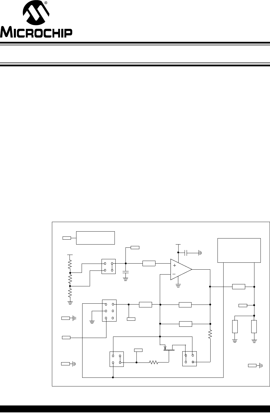
The MCP6XXX Amplifier Evaluation Board 4 is designed to demonstrate an inverting
integrator using one op amp and supporting circuitry. This section details the conver-
sion of the topology to the MCP6XXX Amplifier Evaluation Board 4. Figure 2-1 shows
the circuit diagram for the board.
FIGURE 2-1: MCP6XXX Amplifier Evaluation Board 4 Circuit Diagram.
*
VREF
C3
0.1 µF
RL
U1
VDD
0.1 µF
CU1
CL
2
3
1
2
1
2
1
C1
R2
R3
M1
R4
JP1
JP2
RV1
RV2
RV3
10k
8k
2k
100
100
R1
JP3
Non-Inverting
Comparator
Block
VDD
GND
VL
*
*
Power Supply
Block
Test Point
*
*
*
VIN
VSW
*
VINX
VDD
R5
*
GND
*
GND
*
2
1
JP4
RISO