
User manual


MCP6V01 Input Offset Demo Board User’s Guide
DS51801A-page 6 © 2009 Microchip Technology Inc.
1.3 INTENDED USE
The MCP6V01 Input Offset Demo Board is intended to provide a simple means to
measure the MCP6V01/2/3 op amp’s input offset voltage (V
OS
) under a variety of bias
conditions. This V
OS
includes the specified input offset voltage value found in the data
sheet plus changes due to power supply voltage (PSRR), common mode voltage
(CMRR), output voltage (A
OL
) and temperature (ΔV
OS
/ΔT
A
).
1.4 DESCRIPTION
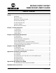
Figure 1-2 shows the block diagram for the MCP6V01 Input Offset Demo Board.
FIGURE 1-2: Block Diagram.
This circuit does the following:
• Supports Microchip’s auto-zeroed, single op amps:
-SOIC-8 package
- Used as both Device Under Test (DUT) and in a difference amplifier
• Test points for connecting lab equipment
• Single supply configuration
• The bias inputs V
DD
, V
CM
and GND set the conditions for the DUT
•The V
DD
/2 Reference uses a resistor ladder to divide V
DD
in half, then buffers that
voltage with an op amp in unity gain
•The V
CM
Reference:
- Has a resistor divider at the input that sets V
CM
=V
DD
/2 when that input is left
open
- When V
CM
is driven by an external voltage source, the resistor divider has no
effect on V
CM
-V
CM
is buffered
• The High Gain Feedback Network and DUT together:
- Have a noise gain of G
N
≈ 10.0 kV/V
- Have a common mode gain of 1 V/V
- Produce an output voltage of G
N
V
OS
+V
CM
Outputs
GND
V
CM
V
DD
GND
V
M
V
DD
/2
Inputs
DUT
Diff. Amp.
V
DD
/2
Reference
V
CM
Reference
(buffered)
(buffered)
High Gain
Feedback
Network
V
REF
.
V
CM