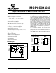
MCP6S91/2/3 Single-Ended, Rail-to-Rail I/O, Low-Gain PGA Features Description • Multiplexed Inputs: 1 or 2 channels • 8 Gain Selections: - +1, +2, +4, +5, +8, +10, +16 or +32 V/V • Serial Peripheral Interface (SPI™) • Rail-to-Rail Input and Output • Low Gain Error: ±1% (max.) • Offset Mismatch Between Channels: 0 µV • High Bandwidth: 1 to 18 MHz (typ.) • Low Noise: 10 nV/√Hz @ 10 kHz (typ.) • Low Supply Current: 1.0 mA (typ.) • Single Supply: 2.5V to 5.
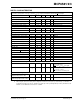
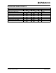
MCP6S91/2/3 1.0 ELECTRICAL CHARACTERISTICS PIN FUNCTION TABLE Name VOUT Absolute Maximum Ratings † Function Analog Output CH0, CH1 Analog Inputs VDD – VSS ........................................................................7.0V VREF External Reference Pin VSS Negative Power Supply Output Short Circuit Current ..................................continuous CS SPI Chip Select Current at Input Pin .............................................................
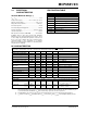
MCP6S91/2/3 DC CHARACTERISTICS (CONTINUED) Electrical Specifications: Unless otherwise indicated, TA = +25°C, VDD = +2.5V to +5.5V, VSS = GND, VREF = VSS, G = +1 V/V, Input = CH0 = (0.3V)/G, CH1 = 0.3V, RL = 10 kΩ to VDD/2, SI and SCK are tied low and CS is tied high. Parameters Sym Min Typ Max Units Conditions Ladder Resistance Ladder Resistance RLAD 3.4 4.9 6.4 kΩ ∆RLAD/∆TA — +0.028 — %/°C DC Output Non-linearity G = +1 VONL — ±0.18 G ≥ +2 VONL — ±0.
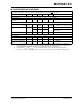
MCP6S91/2/3 AC CHARACTERISTICS Electrical Specifications: Unless otherwise indicated, TA = +25°C, VDD = +2.5V to +5.5V, VSS = GND, VREF = VSS, G = +1 V/V, Input = CH0 = (0.3V)/G, CH1 = 0.3V, RL = 10 kΩ to VDD/2, CL = 60 pF, SI and SCK are tied low and CS is tied high.
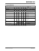
MCP6S91/2/3 DIGITAL CHARACTERISTICS Electrical Specifications: Unless otherwise indicated, TA = 25°C, VDD = +2.5V to +5.5V, VSS = GND, VREF = VSS, G = +1 V/V, Input = CH0 = (0.3V)/G, CH1 = 0.3V, RL = 10 kΩ to VDD/2, CL = 60 pF, SI and SCK are tied low and CS is tied high. Parameters Sym Min Typ Max Units Conditions SPI Inputs (CS, SI, SCK) Logic Threshold, Low VIL 0 — 0.3VDD V Input Leakage Current IIL -1.0 — +1.0 µA Logic Threshold, High VIH 0.
MCP6S91/2/3 TEMPERATURE CHARACTERISTICS Electrical Specifications: Unless otherwise indicated, VDD = +2.5V to +5.5V, VSS = GND.
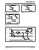
MCP6S91/2/3 CS CS tCH VOUT tG 0.6V FIGURE 1-1: Diagram. 1.5V VOUT 0.3V 0.3V FIGURE 1-3: Diagram. Channel Select Timing Gain Select Timing CS tON tOFF Hi-Z VOUT Hi-Z 0.3V 1.0 mA (typ.) ISS 30 pA (typ.) FIGURE 1-2: PGA Shutdown Timing Diagram (must enter correct commands before CS goes high). tCSH CS tCSSC tSCCS tCS1 tLO tCS0 tHI SCK tSU tHD 1/fSCK SI tDO tSOZ SO (first 16 bits out are always zeros) FIGURE 1-4: Detailed SPI™ Serial Interface Timing; SPI 0,0 Mode.
MCP6S91/2/3 tCSH CS tCSSC tSCCS tCS1 tHI tCS0 tLO SCK tSU tHD 1/fSCK SI tSOZ tDO SO (first 16 bits out are always zeros) FIGURE 1-5: 1.1 Detailed SPI™ Serial Interface Timing; SPI 1,1 Mode. DC Output Voltage Specs / Model 1.1.1 IDEAL MODEL The ideal PGA output voltage (VOUT) is: EQUATION 1-3: EQUATION 1-1: VO_ID = G VIN The end points of this line are at VO_ID = 0.3V and VDD – 0.3V.
MCP6S91/2/3 1.1.4 VOUT (V) VDD V2 VDD – 0.3 DIFFERENT VREF CONDITIONS Some of the plots in Section 2.0 “Typical Performance Curves”, have the conditions VREF = VDD/2 or VREF = VDD. The equations and figures above are easily modified for these conditions. The ideal VOUT equation becomes: O V _LIN O _I D V O_ID = VREF + G ( VIN – VREF ) V DD ≥ V REF > V SS = 0V V V O UT EQUATION 1-7: V1 0.3 0 VIN (V) 0.3 G 0 VDD – 0.
MCP6S91/2/3 2.0 TYPICAL PERFORMANCE CURVES Note: The graphs and tables provided following this note are a statistical summary based on a limited number of samples and are provided for informational purposes only. The performance characteristics listed herein are not tested or guaranteed. In some graphs or tables, the data presented may be outside the specified operating range (e.g., outside specified power supply range) and therefore outside the warranted range.
MCP6S91/2/3 Note: Unless otherwise indicated, TA = +25°C, VDD = +2.5V to +5.5V, VSS = GND, VREF = VSS, G = +1 V/V, Input = CH0 = (0.3V)/G, CH1 = 0.3V, RL = 10 kΩ to VDD/2 and CL = 60 pF. -1 0 1 2 Input Offset Voltage (mV) 35% 25% FIGURE 2-10: σ = 10.0 µVRMS Measurement Repeatability: 10.4 µVRMS 20% 15% 10% 5% 30 20 10 0 -10 -20 0% 3.0 2.5 2.0 1.5 1.0 0.5 0.0 -0.5 -1.0 -1.5 -2.0 -2.5 -3.
MCP6S91/2/3 120 Power Supply Rejection Ratio (dB) 110 100 90 80 70 -50 -25 0 25 50 75 100 125 100 VDD = 2.5V 90 70 60 50 40 30 20 10 100 10 1000 100 PSRR vs. Ambient FIGURE 2-16: 10,000 VDD = 5.5V CH0 = 5.0V 100 MCP6S91 1000000 100k 1M MCP6S92/3 10 PSRR vs. Frequency. MCP6S92/3 VDD = 5.5V 1,000 TA = +125°C 100 TA = +85°C 10 1 1 50 75 100 0.0 0.5 1.0 1.5 2.0 2.5 3.0 3.5 4.0 4.5 5.0 5.5 125 Ambient Temperature (°C) Input Voltage (V) VDD = 5.5V 1.E-09 1n 100p 1.
MCP6S91/2/3 1.2 1.1 1.0 0.9 0.8 0.7 0.6 0.5 0.4 0.3 0.2 0.1 0.0 35 Output Short Circuit Current Magnitude (mA) Quiescent Current (mA) Note: Unless otherwise indicated, TA = +25°C, VDD = +2.5V to +5.5V, VSS = GND, VREF = VSS, G = +1 V/V, Input = CH0 = (0.3V)/G, CH1 = 0.3V, RL = 10 kΩ to VDD/2 and CL = 60 pF. TA = +125°C TA = +85°C TA = +25°C TA = -40°C 30 25 20 10 5 0 0.0 0.5 1.0 1.5 2.0 2.5 3.0 3.5 4.0 4.5 5.0 5.5 Supply Voltage (V) Quiescent Current vs.
MCP6S91/2/3 Note: Unless otherwise indicated, TA = +25°C, VDD = +2.5V to +5.5V, VSS = GND, VREF = VSS, G = +1 V/V, Input = CH0 = (0.3V)/G, CH1 = 0.3V, RL = 10 kΩ to VDD/2 and CL = 60 pF. 40 6 Gain Peaking (dB) 30 Gain (dB) 7 G = +32 G = +16 20 10 0 G = +10 G = +8 G = +5 G = +4 -10 -20 100k 1.E+05 G = +2 G = +1 G = +16 G = +4 G = +1 4 3 2 1 0 1.E+06 1.E+07 1.E+08 1M 10M Frequency (Hz) FIGURE 2-25: 5 10 100M 100 1000 Capacitive Load (pF) FIGURE 2-28: Load. Gain vs. Frequency.
MCP6S91/2/3 Note: Unless otherwise indicated, TA = +25°C, VDD = +2.5V to +5.5V, VSS = GND, VREF = VSS, G = +1 V/V, Input = CH0 = (0.3V)/G, CH1 = 0.3V, RL = 10 kΩ to VDD/2 and CL = 60 pF. 60 300 150 20 100 10 50 GVIN 0 0 -10 -50 VOUT G = +1 G = +5 G = +32 -150 -200 -50 0.200 0.400 0.600 0.800 1.000 1.200 1.400 1.600 1.0 0.0 0.5 1.0 1.5 Time (200 ns/div) Small-Signal Pulse FIGURE 2-34: Response. 0.65 10 5 CS CS 0.45 0 0.40 -5 0.35 -10 VOUT (CH1 = 0.3V, G = +1) 0.
MCP6S91/2/3 1.2 1.1 1.0 0.9 0.8 0.7 0.6 0.5 0.4 0.3 0.2 0.1 0.0 G = 1 V/V VDD = 2.5V 0.0 TA = +125°C TA = +85°C TA = +25°C TA = -40°C 0.5 1.0 Input Offset Voltage (mV) Input Offset Voltage (mV) Note: Unless otherwise indicated, TA = +25°C, VDD = +2.5V to +5.5V, VSS = GND, VREF = VSS, G = +1 V/V, Input = CH0 = (0.3V)/G, CH1 = 0.3V, RL = 10 kΩ to VDD/2 and CL = 60 pF. 1.5 2.0 2.5 Input Voltage (V) Output Voltage Headroom; VDD–VOH and VOL–VSS (mV) G = 1 V/V VDD = 5.
MCP6S91/2/3 3.0 PIN DESCRIPTIONS Descriptions of the pins are listed in Table 3-1. TABLE 3-1: PIN FUNCTION TABLE MCP6S91 MCP6S92 MCP6S93 Symbol 1 1 1 VOUT Analog Output 2 2 2 CH0 Analog Input — 3 3 CH1 Analog Input 3 — 4 VREF External Reference Pin 4 4 5 VSS Negative Power Supply 5 5 6 CS SPI™ Chip Select 6 6 7 SI SPI Serial Data Input — — 8 SO 7 7 9 SCK SPI Clock Input 8 8 10 VDD Positive Power Supply 3.
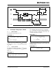
MCP6S91/2/3 4.0 ANALOG FUNCTIONS 4.2 The MCP6S91/2/3 family of Programmable Gain Amplifiers (PGA) is based on simple analog building blocks (see Figure 4-1). Each of these blocks will be explained in more detail in the following subsections. VDD MUX CS SI SO SCK SPI™ Logic VOUT RF 8 Gain Switches RG Resistor Ladder (RLAD) CH0 CH1 VREF VSS MCP6S91 – One input (CH0), no SO pin MCP6S92 – Two inputs (CH0, CH1), VREF tied internally to VSS, no SO pin MCP6S93 – Two inputs (CH0, CH1) FIGURE 4-1: 4.
MCP6S91/2/3 4.2.3 RAIL-TO-RAIL OUTPUT The maximum output voltage swing is the maximum swing possible under a particular amplifier load current. The amplifier load current is the sum of the external load current (IOUT) and the current through the ladder resistance (ILAD); see Figure 4-2. MCP6S9X RIN VIN EQUATION 4-1: RIN ≥ Amplifier Load Current = I OUT + I LAD Where: RIN ≥ ( VOUT – VREF ) I LAD = ------------------------------------RLAD VOUT ILAD RLAD VREF FIGURE 4-2: Amplifier Load Current.
MCP6S91/2/3 4.4 Rail-to-Rail VREF Input The VREF input is intended to be driven by a lowimpedance voltage source. The source driving the VREF pin should have an output impedance less than 0.1Ω to maintain reasonable gain accuracy. The supply voltage VSS and VDD usually meet this requirement. RLAD presents a load at the VREF pin to the external circuit (ZIN_REF ≈ (5 kΩ/G)||(6 pF)), which depends on the gain. Any source driving the VREF pin must be capable of driving a load as heavy as 0.
MCP6S91/2/3 5.0 DIGITAL FUNCTIONS Chain Configuration”, covers applications using multiple 16-bit words. SO goes low after CS goes high; it has a push-pull output that does not go into a high-Z state. The MCP6S91/2/3 PGAs use a standard SPI compatible serial interface to receive instructions from a controller. This interface is configured to allow daisychaining with other SPI devices. 5.1 The MCP6S91/2/3 devices operate in SPI modes 0,0 and 1,1.
MCP6S91/2/3 5.2 Registers The analog functions are programmed through the SPI interface using 16-bit words (see Figure 5-1 and Figure 5-2). This data is sent to two of three 8-bit registers: Instruction register (Register 5-1), Gain register (Register 5-2) and Channel register (Register 5-3). There are no power-up defaults for these three registers. 5.2.1 ENSURING VALID DATA IN THE REGISTERS A 0.1 µF bypass capacitor mounted as close as possible to the VDD pin provides additional transient immunity.
MCP6S91/2/3 5.2.3 SETTING THE GAIN The amplifier can be programmed to produce binary and decimal gain settings between +1 V/V and +32 V/V. Register 5-2 shows the details. At the same time, different compensation capacitors are selected to optimize the bandwidth vs. slew rate trade-off (see Table 4-1).
MCP6S91/2/3 5.2.4 CHANGING THE CHANNEL If the Instruction register is programmed to address the Channel register, the multiplexed inputs of the MCP6S92 and MCP6S93 can be changed using Register 5-3.
MCP6S91/2/3 5.2.5 SHUTDOWN COMMAND The example in Figure 5-3 shows a daisy-chain configuration with two devices, although any number of devices can be configured this way. The MCP6S91 and MCP6S92 can only be used at the far end of the daisychain, because they do not have a serial data out (SO) pin. As shown in Figure 5-4 and Figure 5-5, both SI and SO data are sent in 16-bit (2 byte) words. These devices abort any command that is not a multiple of 16 bits.
MCP6S91/2/3 CS 1 2 3 4 5 6 7 8 9 10111213141516 1 2 3 4 5 6 7 8 9 10111213141516 SCK Instruction Byte for Device 2 Instruction Byte for Device 1 Data Byte for Device 2 bit 0 bit 0 bit 7 bit 0 bit 7 bit 0 bit 7 bit 7 SI Data Byte for Device 1 Instruction Byte for Device 2 FIGURE 5-4: bit 0 bit 0 bit 7 (first 16 bits out are always zeros) bit 7 SO Data Byte for Device 2 Serial Bus Sequence for Daisy-Chain Configuration; SPI™ 0,0 Mode.
MCP6S91/2/3 APPLICATIONS INFORMATION 6.1 Changing External Reference Voltage Figure 6-1 shows a MCP6S91 with the VREF pin at 2.5V and VDD = 5.0V. This allows the PGA to amplify signals centered on 2.5V, instead of ground-referenced signals. The voltage reference MCP1525 is buffered by a MCP6021, which gives a low output impedance reference voltage from DC to high frequencies. The source driving the VREF pin should have an output impedance less than 0.1Ω to maintain reasonable gain accuracy.
MCP6S91/2/3 6.3.2 SUPPLY BYPASS 6.3.4 SIGNAL COUPLING Use a local bypass capacitor (0.01 µF to 0.1 µF) within 2 mm of the VDD pin. It must connect directly to the ground plane. A multi-layer ceramic chip capacitor, or high-frequency equivalent, works best. The input pins of the MCP6S91/2/3 family of PGAs are high-impedance. This makes them especially susceptible to capacitively-coupled noise. Using a ground plane helps reduce this problem. Use a bulk bypass capacitor (2.
MCP6S91/2/3 6.4 Typical Applications VIN 6.4.1 GAIN RANGING MCP6291 Figure 6-5 shows a circuit that measures the current IX. The circuit’s performance benefits from changing the gain on the PGA. Just as a hand-held multimeter uses different measurement ranges to obtain the best results, this circuit makes it easy to set a high gain for small signals and a low gain for large signals. As a result, the required dynamic range at the PGA’s output is less than at its input (by up to 30 dB).
MCP6S91/2/3 6.4.5 6.4.7 EXPANDED INPUT PGA Figure 6-10 shows cascaded MCP6S28 and MCP6S92s PGAs that provide up to 9 input channels. Obviously, Sensors #1-8 have a high total gain range available, as explained in Section 6.4.3 “Extended Gain Range PGA”. These devices can be daisychained (Section 5.3 “Daisy-Chain Configuration”). ADC DRIVER This family of PGAs is well suited for driving Analog-toDigital Converters (ADCs).
MCP6S91/2/3 7.0 PACKAGING INFORMATION 7.1 Package Marking Information 8-Lead PDIP (300 mil) (MCP6S91, MCP6S92) XXXXXXXX XXXXXNNN YYWW MCP6S91 E/P256 0424 8-Lead SOIC (150 mil) (MCP6S91, MCP6S92) XXXXXXXX XXXXYYWW NNN 10-Lead MSOP (MCP6S93) XXXXX YWWNNN Note: * Example: 6S91E 424256 XXXXX YWWNNN XX...
MCP6S91/2/3 8-Lead Plastic Dual In-line (P) – 300 mil (PDIP) E1 D 2 n 1 α E A2 A L c A1 β B1 p eB B Units Dimension Limits n p Number of Pins Pitch Top to Seating Plane Molded Package Thickness Base to Seating Plane Shoulder to Shoulder Width Molded Package Width Overall Length Tip to Seating Plane Lead Thickness Upper Lead Width Lower Lead Width Overall Row Spacing Mold Draft Angle Top Mold Draft Angle Bottom * Controlling Parameter § Significant Characteristic § A A2 A1 E E1 D L c B1 B eB α
MCP6S91/2/3 8-Lead Plastic Small Outline (SN) – Narrow, 150 mil (SOIC) E E1 p D 2 B n 1 α h 45° c A2 A φ β L Units Dimension Limits n p Number of Pins Pitch Overall Height Molded Package Thickness Standoff § Overall Width Molded Package Width Overall Length Chamfer Distance Foot Length Foot Angle Lead Thickness Lead Width Mold Draft Angle Top Mold Draft Angle Bottom * Controlling Parameter § Significant Characteristic A A2 A1 E E1 D h L φ c B α β MIN .053 .052 .004 .228 .146 .189 .010 .
MCP6S91/2/3 8-Lead Plastic Micro Small Outline Package (MS) (MSOP) E p E1 D 2 B n 1 α A2 A c φ A1 (F) L β Number of Pins Pitch Overall Height MILLIMETERS* INCHES Units Dimension Limits n p MAX NOM MIN MIN NOM 0.65 .026 .044 A 1.18 .038 0.76 0.86 .006 0.05 0.97 .193 .200 4.67 4.90 .5.08 .114 .118 .114 .118 .122 2.90 3.00 3.10 .122 2.90 3.00 L .016 3.10 .022 .028 0.40 0.55 .035 Foot Angle F φ 0.70 .037 .039 0.90 0.95 1.
MCP6S91/2/3 10-Lead Plastic Micro Small Outline Package (MS) (MSOP) E E1 p D 2 B n 1 α A φ c A2 A1 L (F) β L1 Units Dimension Limits n p MIN INCHES NOM 10 .020 TYP .033 .193 BSC .118 BSC .118 BSC .024 .037 REF .009 - MAX MILLIMETERS* NOM 10 0.50 TYP. 0.85 0.75 0.00 4.90 BSC 3.00 BSC 3.00 BSC 0.60 0.40 0.95 REF 0° 0.08 0.15 0.23 5° 5° MIN Number of Pins Pitch .043 Overall Height A Molded Package Thickness .037 A2 .030 Standoff .006 A1 .
MCP6S91/2/3 NOTES: 2004 Microchip Technology Inc.
MCP6S91/2/3 PRODUCT IDENTIFICATION SYSTEM To order or obtain information, e.g., on pricing or delivery, refer to the factory or the listed sales office. PART NO.
MCP6S91/2/3 NOTES: DS21908A-page 38 2004 Microchip Technology Inc.
Note the following details of the code protection feature on Microchip devices: • Microchip products meet the specification contained in their particular Microchip Data Sheet. • Microchip believes that its family of products is one of the most secure families of its kind on the market today, when used in the intended manner and under normal conditions. • There are dishonest and possibly illegal methods used to breach the code protection feature.
WORLDWIDE SALES AND SERVICE AMERICAS ASIA/PACIFIC ASIA/PACIFIC EUROPE Corporate Office 2355 West Chandler Blvd. Chandler, AZ 85224-6199 Tel: 480-792-7200 Fax: 480-792-7277 Technical Support: http:\\support.microchip.com Web Address: www.microchip.