
Datasheet


MCP6566/6R/6U/7/9
DS22143D-page 18 2009-2013 Microchip Technology Inc.
It is also possible to connect the diodes to the left of the
resistors R
1
and R
2
. In this case, the currents through
the diodes D
1
and D
2
need to be limited by some other
mechanism. The resistor then serves as in-rush current
limiter; the DC current into the input pins (V
IN
+ and
V
IN
–) should be very small.
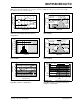
A significant amount of current can flow out of the
inputs when the common mode voltage (V
CM
) is below
ground (V
SS
); see Figure 4-3. Applications that are
high-impedance may need to limit the usable voltage
range.
4.1.3 PHASE REVERSAL
The MCP6566/6R/6U/7/9 comparator family uses
CMOS transistors at the input. They are designed to
prevent phase inversion when the input pins exceed
the supply voltages. Figure 2-3 shows an input voltage
exceeding both supplies with no resulting phase
inversion.
4.2 Open-Drain Output
The open-drain output is designed to make
level-shifting and wired-OR logic easy to implement.
The output stage minimizes switching current
(shoot-through current from supply-to-supply) when
the output changes state. See Figures 2-15, 2-18,
2-35 and 2-36, for more information.
4.3 Externally Set Hysteresis
Greater flexibility in selecting hysteresis (or input trip
points) is achieved by using external resistors.
Hysteresis reduces output chattering when one input is
slowly moving past the other. It also helps in systems
where it is best not to cycle between high and low
states too frequently (e.g., air conditioner thermostatic
control). Output chatter also increases the dynamic
supply current.
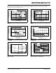
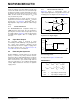
4.3.1 NON-INVERTING CIRCUIT
Figure 4-4 shows a non-inverting circuit for
single-supply applications using just two resistors. The
resulting hysteresis diagram is shown in Figure 4-5.
FIGURE 4-4: Non-Inverting Circuit with
Hysteresis for Single-Supply.
FIGURE 4-5: Hysteresis Diagram for the
Non-Inverting Circuit.
The trip points for Figures 4-4 and 4-5 are:
EQUATION 4-1:
V
REF
V
IN
V
OUT
V
DD
R
1
R
F
+
-
V
PU
R
PU
MCP656X
V
OUT
High-to-Low Low-to-High
V
DD
V
OH
V
OL
V
SS
V
SS
V
DD
V
THL
V
TLH
V
IN
V
TLH
V
REF
1
R
1
R
F
-------+
V
OL
R
1
R
F
-------
–=
V
THL
V
REF
1
R
1
R
F
-------+
V
OH
R
1
R
F
-------
–=
Where:
V
TLH
= trip voltage from low-to-high
V
THL
= trip voltage from high-to-low