
User manual


MCP651 INPUT OFFSET
EVALUATION BOARD
USER’S GUIDE
© 2009 Microchip Technology Inc. DS51834A-page iii
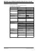
Table of Contents
Preface ........................................................................................................................... 1
Introduction............................................................................................................ 1
Document Layout .................................................................................................. 1
Conventions Used in this Guide ............................................................................ 2
Recommended Reading........................................................................................ 3
The Microchip Web Site ........................................................................................ 3
Customer Support ................................................................................................. 3
Document Revision History................................................................................... 4
Chapter 1. Product Overview
1.1 Introduction ..................................................................................................... 5
1.2 Kit Contents .................................................................................................... 5
1.3 Intended Use .................................................................................................. 6
1.4 Description ..................................................................................................... 6
Chapter 2. Installation and Operation
2.1 Introduction ................................................................................................... 11
2.2 Required Tools ............................................................................................. 11
2.3 Configuring the Lab Equipment and PCB .................................................... 12
2.4 Operating Conditions .................................................................................... 14
2.5 Converting to Other Parameters .................................................................. 15
2.6 Settling Time, Noise and Sampling Rate ...................................................... 17
Chapter 3. Possible Modifications
3.1 Introduction ................................................................................................... 19
3.2 Range of Parts Supported by MCP651 Input Offset Evaluation Board ........ 19
3.3 Changes to Accommodate Other DUTs ....................................................... 21
Appendix A. Schematics and Layouts
A.1 Introduction .................................................................................................. 25
A.2 Schematic and Layouts ................................................................................ 25
A.3 Board – Schematic ....................................................................................... 26
A.4 Board – Combination of the Top Silk Screen, Top Solder Mask and Top Metal
Layers ..................................................................................................... 27
A.5 Board – Top Silk Screen .............................................................................. 28
A.6 Board – Top Solder Mask and Top Metal Layer .......................................... 29
A.7 Board – Bottom Metal Layer ........................................................................ 30