
User manual
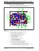


Installation and Operation
© 2009 Microchip Technology Inc. DS51834A-page 15
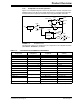
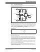
2.5 CONVERTING TO OTHER PARAMETERS
2.5.1 Calculating DUT Parameters
The DUT’s total input offset voltage (V
OST
) can be calculated from a measurement as
shown in Equation 2-1.
EQUATION 2-1:
Changing the DUT’s bias voltages or ambient temperature changes V
OST
. Microchip’s
application note AN1177 discusses in detail how these changes in V
OST
are related to
specifications found in our data sheets. The following list summarizes the results:
• Specified Input Offset Voltage:
-V
OS
= Input offset at the specified bias point
• DC Common Mode Rejection Ratio:
- CMRR = ΔV
CM
/ΔV
OS
• DC Power Supply Rejection Ratio:
- PSRR = (ΔV
DD
– ΔV
SS
)/ΔV
OS
• DC Open-loop Gain:
-A
OL
= ΔV
OUT
/ΔV
OS
• Input Offset Drift over Temperature:
- ΔV
OS
/ΔT
A
Example 2-1 gives an example of how V
OST
changes with the common mode input
voltage (V
CM
).
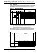
EXAMPLE 2-1: COMMON MODE CHANGE EXAMPLE
V
OST
V
M
G
A
G
M
()
⁄
=
Note: The data sheet Input Offset Voltage (V
OS
) specification applies to one bias
point and temperature only. The total input offset voltage (V
OST
) includes
V
OS
and changes in input offset as bias voltages and temperature change.
Given:
Then:
V
OST
=0.5mV, V
CM
=0V
V
OST
=1.0mV, V
CM
=5V
ΔV
OST
=0.5mV
ΔV
CM
=5.0V
CMRR = 5.0V / 0.5 mV
=10V/mV
=80dB