
User manual


MCP651 Input Offset Evaluation Board User’s Guide
DS51834A-page 12 © 2009 Microchip Technology Inc.
2.3 CONFIGURING THE LAB EQUIPMENT AND PCB
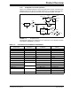
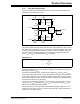
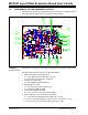
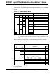
Lab equipment is connected to this board as shown in Figure 2-1. The (surface mount)
test points allow lab equipment to be connected to these boards.
FIGURE 2-1: Lab Equipment Connections and Configuration Switches for the MCP651 Input Offset
Evaluation Board.
The arrows and numbers in Figure 2-1 signify the following:
1. Gain Setting Switch – top position (# 1)
a) To the right (ON) for low gain (G
M
= 201 V/V).
b) To the left for high gain (G
M
=1998V/V).
2. Voltmeter to measure VM
a) Gives amplified offset (G
A
G
M
V
OST
).
3. Power Supply for VCOX
a) Can be left open (forces VOUTX = 0V).
b) Set between VSSI and VDDI.
4. ±2.5V Power Supplies with GND
a) Set at +2.5V and -2.5V (for best performance).
5. Power Supply for VLX (Load Resistor’s bias point)
a) Can be left open (fewer lab power supplies; R
L
=40kΩ).
b) Can be shorted to GND with a jumper wire (VLX = 0V and R
L
=1kΩ).
c) Can connect to an external lab power supply (R
L
=1kΩ).
4
1
2
3
5 6
7
8
9
10
11
1213