
User manual


MCP651 Input Offset Evaluation Board User’s Guide
DS51834A-page 10 © 2009 Microchip Technology Inc.
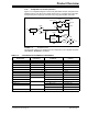
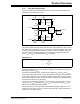
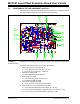
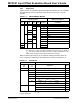
1.4.4 CAL Input
The DUT’s CAL/CS input pin is normally held at V
SSX
by resistors R
20
and R
21
; this
keeps the MCP651 in its normal mode of operation. When S
1
is closed by the user, R
20
pulls CAL/CS
up to V
DDX
(after a time set by R
20
and C
9
), so that the MCP651 enters
its low power mode of operation. Releasing S
1
then brings CAL/CS back to V
SSX
(after
a time set by R
20
, R
21
and C
9
); the time constant (R
20
+R
21
)C
9
is 0.11s, which is slow
enough to de-glitch S
1
. Note that the supply voltages need to be constant while the
DUT is being put into calibration mode, and during calibration mode (up to 4 ms of time
after CAL/CS
goes low).
FIGURE 1-4: CAL Switch and De-glitching Circuitry.
1.4.5 Bias Inputs for Other Op Amps
The other op amps (U
2
, U
3
and U
4
) are run on dual power supplies centered on ground.
The design assumes that these supplies are ±2.5V, for the best performance. These
supplies can be set as low as ±0.9V, which will keep the MCP6V01’s working, but will
reduce the range of possible V
COX
and V
M
values.
1.4.6 Outputs
The connector V
CALX
outputs the voltage set by the POT RCAL. V
DDI
and V
SSI
are
used to measure the actual DUT supply voltages, and to estimate its supply currents
I
DD
and I
SS
. V
OUTX
is the DUT’s output voltage; it is used only to verify that the circuit
is operating correctly. V
M
is the most important output; it is V
OST
multiplied by either
201 V/V or 1998 V/V.
C
9
R
21
10 kΩ
R
37
R
29
4.49Ω
4.99Ω
V
DDX
1.0 µF
DUT
CAL/CS
U
1
V
SS
V
DD
R
38
R
30
4.49Ω
4.99Ω
V
SSX
S
1
R
41
10Ω
R
19
10 kΩ
R
20
100 kΩ