
User manual


Product Overview
© 2009 Microchip Technology Inc. DS51834A-page 7
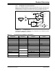
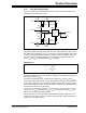
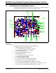
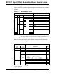
1.4.2 Simplified Circuit and Operation
Figure 1-2 is a simplified diagram of the circuitry that biases the DUT and produces an
amplified version of the DUT’s input offset voltage (V
OST
). It includes gain at the input,
a Proportional plus Integral (PI) controller loop, a high gain amplifier and a filter.
FIGURE 1-2: Simplified Circuit.
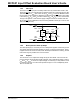
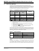
The elements of Figure 1-2 correspond to the components in the complete schematic
(A.3 “Board – Schematic”) as follows.
TABLE 1-2: CONVERSION OF SCHEMATIC COMPONENTS
DUT
V
OUTX
R
12
R
56
V
CMX
=0V
R
3
R
4
Integrator
1/G
INT
(ω
INT
/s)
G
M
V
M
V
DDI
V
SSI
1/G
INT
C
2
+2.5V
-2.5V
+2.5V
-2.5V
V
COX
+1
+2.5V
-2.5V
R
78
Lowpass
Filter
Complete Schematic
Components
Simplified Schematic
Component
Conversion
Equations
Typical Values
(Note 1)
R1, R2 R
12
=R1||R2 ≈ 196.1Ω
R3 R
3
=R3 ≈ 200.0Ω
R4 R
4
=R4 ≈ 10.00 kΩ
R5, R6 R
56
=R5+R6 ≈ 8.04 kΩ
R7, R8 R
78
=R7+R8 ≈ 40.0 kΩ
C2 C
2
=C2 ≈ 22 nF
U1 “DUT” — —
U2 “+1 Buffer” — —
R11, R12 “1/G
INT
” = R11 / (R11 + R12) ≈ 1 / (3.213 V/V)
R13, R14 = R13 / (R13 + R14) ≈ 1 / (3.213 V/V)
U3, R11, R12, C6 “Integrator (ω
INT
/s)” ω
INT
= 1 / ((R11 || R12)C6) ≈ 2π (10.3 Hz)
U3, R17, C7 ω
INT
= 1 / (R17 · C7) ≈ 2π (10.4 Hz)
U4, R23, R24, R25, R26, S2 “G
M
” =1+R24/R23 ≈ 3.941 V/V, S2 closed
= 1 + (R24 + R25 + R26) / R23 ≈ 39.18V/V, S2open
R28, C12 “Lowpass Filter (ω
BW
)” ω
BW
= 1 / (R28 · C12) ≈ 2π (1.59 Hz)
Note 1: Switch S2’s top position is closed when to the right (LOW GAIN), and is open when to the left (HI GAIN).