MCP651 Input Offset Evaluation Board User’s Guide © 2009 Microchip Technology Inc.
Note the following details of the code protection feature on Microchip devices: • Microchip products meet the specification contained in their particular Microchip Data Sheet. • Microchip believes that its family of products is one of the most secure families of its kind on the market today, when used in the intended manner and under normal conditions. • There are dishonest and possibly illegal methods used to breach the code protection feature.
MCP651 INPUT OFFSET EVALUATION BOARD USER’S GUIDE Table of Contents Preface ........................................................................................................................... 1 Introduction............................................................................................................ 1 Document Layout .................................................................................................. 1 Conventions Used in this Guide .......................................
MCP651 Input Offset Evaluation Board User’s Guide Appendix B. Bill Of Materials (BOM) B.1 MCP651 Input Offset Evaluation Board BOM .............................................. 31 B.2 Adaptor Board BOM ..................................................................................... 33 Worldwide Sales and Service .....................................................................................34 DS51834A-page iv © 2009 Microchip Technology Inc.
MCP651 INPUT OFFSET EVALUATION BOARD USER’S GUIDE Preface NOTICE TO CUSTOMERS All documentation becomes dated, and this manual is no exception. Microchip tools and documentation are constantly evolving to meet customer needs, so some actual dialogs and/or tool descriptions may differ from those in this document. Please refer to our web site (www.microchip.com) to obtain the latest documentation available. Documents are identified with a “DS” number.
MCP651 Input Offset Evaluation Board User’s Guide CONVENTIONS USED IN THIS GUIDE This manual uses the following documentation conventions: DOCUMENTATION CONVENTIONS Description Arial font: Italic characters Represents Referenced books Emphasized text A window A dialog A menu selection A field name in a window or dialog A menu path MPLAB® IDE User’s Guide ...is the only compiler...
Preface RECOMMENDED READING This user's guide describes how to use MCP651 Input Offset Evaluation Board. Other useful documents are listed below. The following Microchip documents are available and recommended as supplemental reference resources. MCP6V01/2/3 Data Sheet, “300 µA, Auto-Zeroed Op Amps”, DS22058 Gives detailed information on the op amp family that is used for signal processing and output voltage control on the MCP651 Input Offset Evaluation Board.
MCP651 Input Offset Evaluation Board User’s Guide DOCUMENT REVISION HISTORY Revision A (May 2009) • Initial Release of this Document. DS51834A-page 4 © 2009 Microchip Technology Inc.
MCP651 INPUT OFFSET EVALUATION BOARD USER’S GUIDE Chapter 1. Product Overview 1.1 INTRODUCTION The MCP651 Input Offset Evaluation Board is described by the following: • Assembly # : 102-00258-R2 • Order # : MCP651EV-VOS • Name: MCP651 Input Offset Evaluation Board Items discussed in this chapter include: • Kit Contents • Intended Use • Description 1.2 KIT CONTENTS • One MCP651 Input Offset Evaluation Board, 102-00258-R2 • Important Information “Read First” FIGURE 1-1: © 2009 Microchip Technology Inc.
MCP651 Input Offset Evaluation Board User’s Guide 1.3 INTENDED USE The MCP651 Input Offset Evaluation Board is intended to provide a simple means to measure the MCP651 Input Offset Evaluation Board op amp’s input offset voltage under a variety of operating conditions.
Product Overview 1.4.2 Simplified Circuit and Operation Figure 1-2 is a simplified diagram of the circuitry that biases the DUT and produces an amplified version of the DUT’s input offset voltage (VOST). It includes gain at the input, a Proportional plus Integral (PI) controller loop, a high gain amplifier and a filter. VCMX = 0V VDDI R12 R3 DUT R4 R78 VOUTX VSSI +2.5V VM Lowpass Filter GM R56 +2.5V -2.5V C2 1/GINT Integrator (ωINT/s) +2.5V 1/GINT -2.5V FIGURE 1-2: VCOX +1 -2.
MCP651 Input Offset Evaluation Board User’s Guide Analysis of this simplified circuit gives the following nominal circuit outputs: EQUATION 1-2: V OUTX ≈ V COX V M ≈ G A G M V OST Where: GA = 1 + R4/R3 ≈ 51.00 V/V GAGM ≈ 201.0 V/V, S2 (position 1) closed ≈ 1998 V/V, S2 (position 1) open R1 and R2 (R12) balance the circuit at the DUT’s input. These resistors are small, and are oriented on the Printed Circuit Board (PCB) to cancel their thermoelectric voltages.
Product Overview 1.4.3 DUT Bias Voltage Inputs Figure 1-3 shows the basic DUT biasing circuitry, except the input pins which have already been discussed (VCMX = 0V). R37 4.49Ω R29 4.49Ω VDDI VDDX C21 10 µF R44 2.2 kΩ VCALX R43 10 kΩ R42 150Ω C13 100 nF IDD DUT U1 VDD C25 100 nF C22 10 µF VCAL VOUT VSS C14 100 nF FIGURE 1-3: VOUTX VLX ISS VSSX R38 4.49Ω R10 1.00 kΩ R30 4.49Ω VSSI DUT Bias Circuitry. Lab power supplies are connected to VDDX and VSSX.
MCP651 Input Offset Evaluation Board User’s Guide 1.4.4 CAL Input The DUT’s CAL/CS input pin is normally held at VSSX by resistors R20 and R21; this keeps the MCP651 in its normal mode of operation. When S1 is closed by the user, R20 pulls CAL/CS up to VDDX (after a time set by R20 and C9), so that the MCP651 enters its low power mode of operation. Releasing S1 then brings CAL/CS back to VSSX (after a time set by R20, R21 and C9); the time constant (R20 + R21)C9 is 0.
MCP651 INPUT OFFSET EVALUATION BOARD USER’S GUIDE Chapter 2. Installation and Operation 2.1 INTRODUCTION This chapter shows how to set up and operate the MCP651 Input Offset Evaluation Board. Items discussed in this chapter include: • • • • • 2.2 Required Tools Configuring the Lab Equipment and PCB Operating Conditions Calculating DUT Parameters Settling Time, Noise, and Sampling Rate REQUIRED TOOLS • (1 or 2) Lab Power Supplies with (two) tracking outputs - One for +2.5V, GND -2.
MCP651 Input Offset Evaluation Board User’s Guide 2.3 CONFIGURING THE LAB EQUIPMENT AND PCB Lab equipment is connected to this board as shown in Figure 2-1. The (surface mount) test points allow lab equipment to be connected to these boards. 13 12 11 1 10 2 9 3 8 7 4 FIGURE 2-1: Evaluation Board. 5 6 Lab Equipment Connections and Configuration Switches for the MCP651 Input Offset The arrows and numbers in Figure 2-1 signify the following: 1.
Installation and Operation 6. Voltmeter to measure VOUTX a) Typically not used (mainly used for validating DUT and board). 7. POT (RCAL) Thumb-wheel (to adjust VCALX) a) Rotate clockwise (CW) to increase VCALX. b) Rotate counter-clockwise (CCW) to decrease VCALX. c) Usually set at mid-turn. d) Can override with an external power supply at VCALX or a jumper wire (see # 9 below) 8. Power Supply for VSSX a) Minimum of about VDDX – (DUT’s maximum operating supply voltage) – (0.
MCP651 Input Offset Evaluation Board User’s Guide 2.4 OPERATING CONDITIONS The MCP651 Input Offset Evaluation Board works most effectively at room temperature (near 25°C). Measurements at other temperatures should be done in an oven where the air velocity is minimal. Table 2-1 shows the various DUT voltages (as described in the data sheet), their nominal values and ranges, and how to convert to the voltages needed on the MCP651 Input Offset Evaluation Board.
Installation and Operation 2.5 CONVERTING TO OTHER PARAMETERS 2.5.1 Calculating DUT Parameters The DUT’s total input offset voltage (VOST) can be calculated from a measurement as shown in Equation 2-1. EQUATION 2-1: V OST = V M ⁄ ( G A G M ) Changing the DUT’s bias voltages or ambient temperature changes VOST. Microchip’s application note AN1177 discusses in detail how these changes in VOST are related to specifications found in our data sheets.
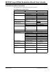
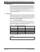
MCP651 Input Offset Evaluation Board User’s Guide 2.5.2 Application Table 2-3 shows one possible measurement matrix that will allow the user to estimate key parameters for the DUT. Obviously, other values of VDD and VCAL could be selected. TABLE 2-3: MEASUREMENT MATRIX Operating Inputs TA (°C) VDD (V) VOUT (V) +25 5.5 2.75 VCM (V) GM (V/V) Symbol 1.83 40 VM1 VOS and PSRR -0.30 4 VM2 CMRR 4.20 VM3 CMRR 1.83 VM4 AOL VM5 AOL 0.20 5.30 2.5 1.25 0.
Installation and Operation 2.6 SETTLING TIME, NOISE AND SAMPLING RATE The bandwidth seen by the signal (DUT’s VOST and noise voltage), between the DUT’s input and VM, is set mainly by the lowpass filter at the VM test point (TP5); this bandwidth is about 1.6 Hz. This bandwidth sets the settling time seen at VM (after the DUT’s bias point has been changed) to about 0.6 seconds. The noise seen in the measurements is a result of DUT’s input noise voltage passed through the same 1.6 Hz lowpass filter.
MCP651 Input Offset Evaluation Board User’s Guide NOTES: DS51834A-page 18 © 2009 Microchip Technology Inc.
MCP651 INPUT OFFSET EVALUATION BOARD USER’S GUIDE Chapter 3. Possible Modifications 3.1 INTRODUCTION This chapter shows how to modify the MCP651 Input Offset Evaluation Board to measure other single op amps from Microchip Technology Inc. Items discussed in this chapter include: • Range of Parts Supported by the MCP651 Input Offset Evaluation Board • Changes to Accommodate Other DUTs 3.
MCP651 Input Offset Evaluation Board User’s Guide 3.2.2 Output Headroom The DUT’s output headroom needs to be close enough to 0V to not overdrive U2 or U3. The maximum DUT VOH and VOL values supported (relative to VCM) are: EQUATION 3-2: V OH – V CM ≤ 7.5V V CM – V OL ≤ 7.5V Rail-to-rail output op amps, on a single supply voltage, must be less than 7.5V. 3.2.
Possible Modifications 3.3 CHANGES TO ACCOMMODATE OTHER DUTS This section focuses on methods to connect to other DUTs; the circuit’s design is not changed. Parts information can be found in Appendix B. “Bill Of Materials (BOM)”. 3.3.1 Pinout Figure 3-1 shows the MCP651 op amp’s pinout. This is the standard 8-lead pinout, except for pins 5 and 8 (VCAL and CAL/CS).
MCP651 Input Offset Evaluation Board User’s Guide 3.3.3 Single Op Amps in SOIC-8 Package Solder onto the SOIC-8 pad shown in Figure 3-2. Pin 1 is on the top left (next to the U1 label). To avoid soldering and de-soldering many times, for slower parts, it may be better to use the option discussed in Section 3.3.5 “Other Single Op Amps”. 3.3.4 Single Op Amps in PDIP-8 Package Remove the original SOIC-8 packaged part.
Possible Modifications Figure 3-4 shows a SOIC-8 op amp soldered onto the 8-Pin SOIC/MSOP/TSSOP/DIP Evaluation Board available from Microchip Technology Inc. The two interconnect strips on the bottom are soldered into the through holes for the DIP-8 socket. Figure 3-5 shows this board plugged into the MCP651 Input Offset Evaluation Board. Note 1: 2: Build the adaptor board in the following sequence. Insert the interconnect headers into the DIP-8 socket on the MCP651 Input Offset Evaluation Board.
MCP651 Input Offset Evaluation Board User’s Guide NOTES: DS51834A-page 24 © 2009 Microchip Technology Inc.
MCP651 INPUT OFFSET EVALUATION BOARD USER’S GUIDE Appendix A. Schematics and Layouts A.1 INTRODUCTION This appendix contains the schematics and layouts for the MCP651 Input Offset Evaluation Board. A.2 SCHEMATIC AND LAYOUTS See A.3 “Board – Schematic” for the circuit diagram. U1 is the DUT (MCP651). U2 buffers the attenuated and filtered control voltage VCOX. U3 is the differential integrator. U4 is the amplifier that gives the final gain to the DUT’s input offset voltage (VOST).
MCP651 Input Offset Evaluation Board User’s Guide BOARD – SCHEMATIC M A.3 DS51834A-page 26 © 2009 Microchip Technology Inc.
Schematics and Layouts A.4 BOARD – COMBINATION OF THE TOP SILK-SCREEN, TOP SOLDER MASK AND TOP METAL LAYERS © 2009 Microchip Technology Inc.
MCP651 Input Offset Evaluation Board User’s Guide A.5 BOARD – TOP SILK-SCREEN DS51834A-page 28 © 2009 Microchip Technology Inc.
Schematics and Layouts A.6 BOARD – TOP SOLDER MASK AND TOP METAL LAYER © 2009 Microchip Technology Inc.
MCP651 Input Offset Evaluation Board User’s Guide A.7 BOARD – BOTTOM METAL LAYER DS51834A-page 30 © 2009 Microchip Technology Inc.
MCP651 INPUT OFFSET EVALUATION BOARD USER’S GUIDE Appendix B. Bill Of Materials (BOM) B.1 MCP651 INPUT OFFSET EVALUATION BOARD BOM The BOM in Table B-1 shows all of the components assembled on the PCB. Table B-2 shows alternate components that can be placed on this PCB (after modification). Table B-3 shows components that are not populated. TABLE B-1: BILL OF MATERIALS FOR ASSEMBLED PCB Reference Designator Qty Description Manufacturer Part Number 1 C8 1.
Bill Of Materials (BOM) Reference Designator Qty Description Manufacturer Part Number 5 R32 – R34, R39, R41 10Ω, 1206 SMD, 5%, 1/4W Panasonic-ECG ERJ-8GEYJ100V 1 R42 150Ω, 1206 SMD, 5%, 1/4W Panasonic-ECG ERJ-8GEYJ151V 1 R44 2.2 kΩ, 1206 SMD, 5%, 1/4W Panasonic-ECG ERJ-8GEYJ222V 1 R43 10 kΩ POT, SMD, 20%, 1 Turn Thumbwheel Bournes Inc. 3352T-1-103LF 1 S1 SPST-NO, SMD, Switch, Push Button, 1 Pos. Panasonic-ECG EVQ-P2R02M 1 S2 SMD, Switch, DIP, 2 Pos. Grayhill Inc.
Bill Of Materials (BOM) B.2 ADAPTOR BOARD BOM The BOM in Table B-4 shows the components needed to build the adaptor board for alternate DUT’s (see Figure 3-4). TABLE B-4: BILL OF MATERIALS FOR ADAPTOR BOARD Qty Reference Designator 1 — 8-Pin SOIC/MSOP/TSSOP/DIP Evaluation Board Microchip Technology SOIC8EV Inc. 2 — Board-to-Board Connector, Low Profile Header, 4 Positions, 0.100 in, Gold Plated Samtec Inc.
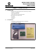
WORLDWIDE SALES AND SERVICE AMERICAS ASIA/PACIFIC ASIA/PACIFIC EUROPE Corporate Office 2355 West Chandler Blvd. Chandler, AZ 85224-6199 Tel: 480-792-7200 Fax: 480-792-7277 Technical Support: http://support.microchip.com Web Address: www.microchip.