
Datasheet


Table Of Contents
- Package Types
- Typical Application
- 1.0 Electrical Characteristics
- 2.0 Typical Performance Curves
- Figure 2-1: Input Offset Voltage
- Figure 2-2: Input Offset Voltage Drift
- Figure 2-3: Input Offset Voltage vs. Common Mode Input Voltage
- Figure 2-4: Input Offset Voltage vs. Common Mode Input Voltage
- Figure 2-5: Input Offset Voltage vs. Output Voltage
- Figure 2-6: Input Offset Voltage vs. Power Supply Voltage
- FIGURE 2-7: Input Noise Voltage Density vs. Frequency.
- FIGURE 2-8: Input Noise Voltage Density vs. Common Mode Input Voltage.
- FIGURE 2-9: CMRR, PSRR vs. Frequency.
- FIGURE 2-10: CMRR, PSRR vs. Ambient Temperature.
- FIGURE 2-11: Input Bias, Offset Currents vs. Ambient Temperature.
- FIGURE 2-12: Input Bias Current vs. Common Mode Input Voltage.
- FIGURE 2-13: Quiescent Current vs. Ambient Temperature.
- FIGURE 2-14: Quiescent Current vs. Common Mode Input Voltage.
- FIGURE 2-15: Quiescent Current vs. Common Mode Input Voltage.
- FIGURE 2-16: Quiescent Current vs. Power Supply Voltage.
- FIGURE 2-17: Open-Loop Gain, Phase vs. Frequency.
- FIGURE 2-18: DC Open-Loop Gain vs. Ambient Temperature.
- FIGURE 2-19: Gain Bandwidth Product, Phase Margin vs. Ambient Temperature.
- FIGURE 2-20: Gain Bandwidth Product, Phase Margin vs. Ambient Temperature.
- FIGURE 2-21: Output Short Circuit Current vs. Power Supply Voltage.
- FIGURE 2-22: Output Voltage Swing vs. Frequency.
- FIGURE 2-23: Output Voltage Headroom vs. Output Current.
- FIGURE 2-24: Output Voltage Headroom vs. Output Current.
- FIGURE 2-25: Output Voltage Headroom vs. Ambient Temperature.
- FIGURE 2-26: Output Voltage Headroom vs. Ambient Temperature.
- FIGURE 2-27: Slew Rate vs. Ambient Temperature.
- FIGURE 2-28: Small Signal Non-Inverting Pulse Response.
- FIGURE 2-29: Small Signal Inverting Pulse Response.
- FIGURE 2-30: Large Signal Non-Inverting Pulse Response.
- FIGURE 2-31: Large Signal Inverting Pulse Response.
- FIGURE 2-32: The MCP6491/2/4 Shows No Phase Reversal.
- FIGURE 2-33: Closed Loop Output Impedance vs. Frequency.
- FIGURE 2-34: Measured Input Current vs. Input Voltage (below VSS).
- FIGURE 2-35: Channel-to-Channel Separation vs. Frequency (MCP6492/4 only).
- 3.0 Pin Descriptions
- 4.0 Application Information
- 5.0 Design Aids
- 6.0 Packaging Information
- Appendix A: Revision History
- Product Identification System
- Trademarks
- Worldwide Sales and Service
2012-2013 Microchip Technology Inc. DS20002321C-page 7
MCP6491/2/4
2.0 TYPICAL PERFORMANCE CURVES
Note: Unless otherwise indicated, T
A
=+25°C, V
DD
= +2.4V to +5.5V, V
SS
= GND, V
CM
=V
DD
/2, V
OUT
V
DD
/2,
V
L
=V
DD
/2, R
L
=10kto V
L
and C
L
=20pF.
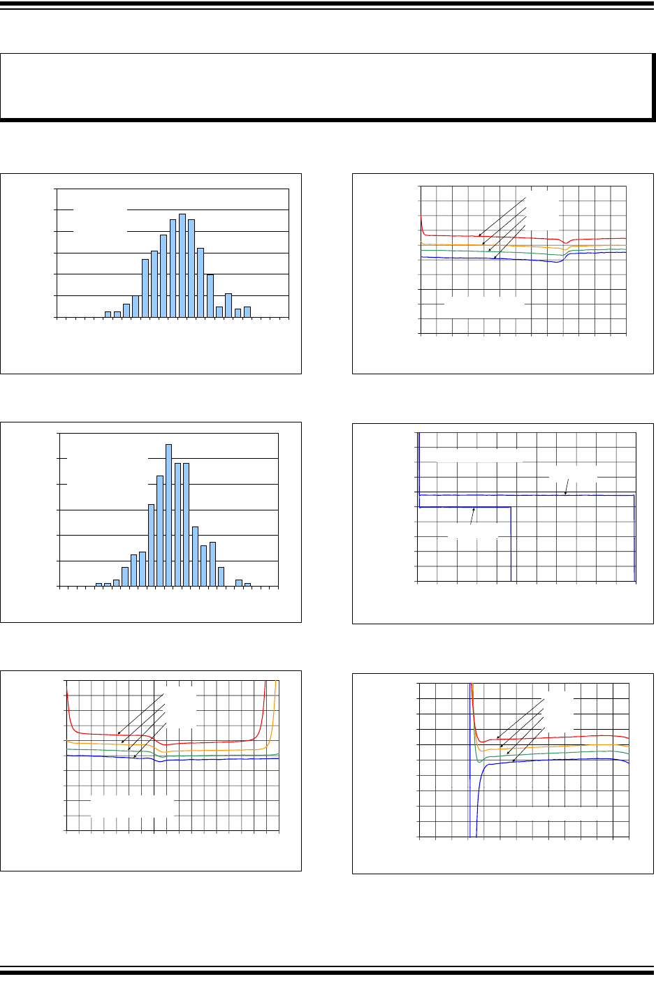
FIGURE 2-1: Input Offset Voltage.
FIGURE 2-2: Input Offset Voltage Drift.
FIGURE 2-3: Input Offset Voltage vs.
Common Mode Input Voltage.
FIGURE 2-4: Input Offset Voltage vs.
Common Mode Input Voltage.
FIGURE 2-5: Input Offset Voltage vs.
Output Voltage.
FIGURE 2-6: Input Offset Voltage vs.
Power Supply Voltage.
Note: The graphs and tables provided following this note are a statistical summary based on a limited number of
samples and are provided for informational purposes only. The performance characteristics listed herein
are not tested or guaranteed. In some graphs or tables, the data presented may be outside the specified
operating range (e.g., outside specified power supply range) and therefore outside the warranted range.
0%
3%
6%
9%
12%
15%
18%
-1200
-1000
-800
-600
-400
-200
0
200
400
600
800
1000
1200
Percentage of Occurrences
Input Offset Voltage (µV)
270 Samples
V
DD
= 3.0V
V
CM
= V
DD
/4
0%
3%
6%
9%
12%
15%
18%
-12
-10
-8
-6
-4
-2
0
2
4
6
8
10
12
Percentage of Occurrences
Input Offset Voltage Drift (µV/°C)
270 Samples
V
DD
= 3.0V
V
CM
= V
DD
/4
T
A
= -40°C to +125°C
-
400
-200
0
200
400
600
800
1000
u
t Offset Voltage (µV)
+125°C
+85°C
+25°C
-40°C
-1000
-800
-600
-
400
-0.5
-0.3
-0.1
0.1
0.3
0.5
0.7
0.9
1.1
1.3
1.5
1.7
1.9
2.1
2.3
2.5
2.7
2.9
Inp
u
Common Mode Input Voltage (V)
V
DD
= 2.4V
Representative Part
-
400
-200
0
200
400
600
800
1000
u
t Offset Voltage (µV)
+125°C
+85°C
+25°C
-40°C
-1000
-800
-600
-
400
-0.5
0.0
0.5
1.0
1.5
2.0
2.5
3.0
3.5
4.0
4.5
5.0
5.5
6.0
Inp
u
Common Mode Input Voltage (V)
V
DD
= 5.5V
Representative Part
-
400
-200
0
200
400
600
800
1000
t
Offset Voltage (µV)
V
DD
= 5.5V
V
DD
= 2.4V
Representative Part
-1000
-800
-600
400
0.0
0.5
1.0
1.5
2.0
2.5
3.0
3.5
4.0
4.5
5.0
5.5
Inpu
t
Output Voltage (V)
400
-200
0
200
400
600
800
1000
t
Offset Voltage (µV)
+125°C
+85°C
+25°C
-40°C
-1000
-800
-600
-
400
0.0
0.5
1.0
1.5
2.0
2.5
3.0
3.5
4.0
4.5
5.0
5.5
6.0
6.5
Inpu
t
Power Supply Voltage (V)
Representative Part