
Datasheet


Table Of Contents
- Package Types
- Typical Application
- 1.0 Electrical Characteristics
- 2.0 Typical Performance Curves
- Figure 2-1: Input Offset Voltage
- Figure 2-2: Input Offset Voltage Drift
- Figure 2-3: Input Offset Voltage vs. Common Mode Input Voltage
- Figure 2-4: Input Offset Voltage vs. Common Mode Input Voltage
- Figure 2-5: Input Offset Voltage vs. Output Voltage
- Figure 2-6: Input Offset Voltage vs. Power Supply Voltage
- FIGURE 2-7: Input Noise Voltage Density vs. Frequency.
- FIGURE 2-8: Input Noise Voltage Density vs. Common Mode Input Voltage.
- FIGURE 2-9: CMRR, PSRR vs. Frequency.
- FIGURE 2-10: CMRR, PSRR vs. Ambient Temperature.
- FIGURE 2-11: Input Bias, Offset Currents vs. Ambient Temperature.
- FIGURE 2-12: Input Bias Current vs. Common Mode Input Voltage.
- FIGURE 2-13: Quiescent Current vs. Ambient Temperature.
- FIGURE 2-14: Quiescent Current vs. Common Mode Input Voltage.
- FIGURE 2-15: Quiescent Current vs. Common Mode Input Voltage.
- FIGURE 2-16: Quiescent Current vs. Power Supply Voltage.
- FIGURE 2-17: Open-Loop Gain, Phase vs. Frequency.
- FIGURE 2-18: DC Open-Loop Gain vs. Ambient Temperature.
- FIGURE 2-19: Gain Bandwidth Product, Phase Margin vs. Ambient Temperature.
- FIGURE 2-20: Gain Bandwidth Product, Phase Margin vs. Ambient Temperature.
- FIGURE 2-21: Output Short Circuit Current vs. Power Supply Voltage.
- FIGURE 2-22: Output Voltage Swing vs. Frequency.
- FIGURE 2-23: Output Voltage Headroom vs. Output Current.
- FIGURE 2-24: Output Voltage Headroom vs. Output Current.
- FIGURE 2-25: Output Voltage Headroom vs. Ambient Temperature.
- FIGURE 2-26: Output Voltage Headroom vs. Ambient Temperature.
- FIGURE 2-27: Slew Rate vs. Ambient Temperature.
- FIGURE 2-28: Small Signal Non-Inverting Pulse Response.
- FIGURE 2-29: Small Signal Inverting Pulse Response.
- FIGURE 2-30: Large Signal Non-Inverting Pulse Response.
- FIGURE 2-31: Large Signal Inverting Pulse Response.
- FIGURE 2-32: The MCP6491/2/4 Shows No Phase Reversal.
- FIGURE 2-33: Closed Loop Output Impedance vs. Frequency.
- FIGURE 2-34: Measured Input Current vs. Input Voltage (below VSS).
- FIGURE 2-35: Channel-to-Channel Separation vs. Frequency (MCP6492/4 only).
- 3.0 Pin Descriptions
- 4.0 Application Information
- 5.0 Design Aids
- 6.0 Packaging Information
- Appendix A: Revision History
- Product Identification System
- Trademarks
- Worldwide Sales and Service
MCP6491/2/4
DS20002321C-page 18 2012-2013 Microchip Technology Inc.
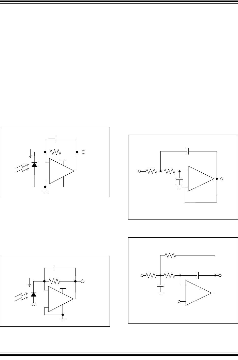
4.7 Application Circuits
4.7.1 PHOTO DETECTION
The MCP6491/2/4 op amps can be used to easily
convert the signal from a sensor that produces an
output current (such as a photo diode) into a voltage (a
transimpedance amplifier). This is implemented with a
single resistor (R
2
) in the feedback loop of the
amplifiers shown in Figure 4-8 and Figure 4-9. The
optional capacitor (C
2
) sometimes provides stability for
these circuits.
A photodiode configured in the Photovoltaic mode has
zero voltage potential placed across it (Figure 4-8). In
this mode, the light sensitivity and linearity is
maximized, making it best suited for precision
applications. The key amplifier specifications for this
application are: low-input bias current, Common mode
input voltage range (including ground), and rail-to-rail
output.
FIGURE 4-8: Photovoltaic Mode Detector.
In contrast, a photodiode that is configured in the
Photoconductive mode has a reverse bias voltage
across the photo-sensing element (Figure 4-9). This
decreases the diode capacitance, which facilitates
high-speed operation (e.g., high-speed digital
communications). However, the reverse bias voltage
also increased diode leakage current and caused
linearity errors.
FIGURE 4-9: Photoconductive Mode
Detector.
4.7.2 ACTIVE LOW PASS FILTER
The MCP6491/2/4 op amps’ low-input bias current
makes it possible for the designer to use larger
resistors and smaller capacitors for active low-pass
filter applications. However, as the resistance
increases, the noise generated also increases.
Parasitic capacitances and the large value resistors
could also modify the frequency response. These
trade-offs need to be considered when selecting circuit
elements.
Usually, the op amp bandwidth is 100x the filter cutoff
frequency (or higher) for good performance. It is
possible to have the op amp bandwidth 10x higher than
the cutoff frequency, thus having a design that is more
sensitive to component tolerances.
Figure 4-10 and Figure 4-11 show low-pass, second-
order, Butterworth filters with a cutoff frequency of
10 Hz. The filter in Figure 4-10 has a non-inverting gain
of +1 V/V, and the filter in Figure 4-11 has an inverting
gain of -1 V/V.
FIGURE 4-10: Second-Order, Low-Pass
Butterworth Filter with Sallen-Key Topology.
FIGURE 4-11: Second-Order, Low-Pass
Butterworth Filter with Multiple-Feedback
Topology.
D
1
Light
V
OUT
V
DD
R
2
C
2
I
D1
V
OUT
= I
D1
*R
2
–
+
MCP6491
D
1
Light
V
OUT
V
DD
R
2
C
2
I
D1
V
OUT
= I
D1
*R
2
V
BIAS
V
BIAS
< 0V
–
+
MCP6491
C
2
V
OUT
R
1
R
2
C
1
V
IN
47 nF
768 k
1.27 M
22 nF
f
P
= 10 Hz, G = +1 V/V
+
–
MCP6491
C
2
V
OUT
R
1
R
3
C
1
V
IN
R
2
V
DD
/2
f
P
= 10 Hz, G = -1 V/V
618 k
618 k
1.00 M
8.2 nF
47 nF
–
+
MCP6491