
Datasheet


Table Of Contents
- Package Types
- Typical Application
- 1.0 Electrical Characteristics
- 2.0 Typical Performance Curves
- Figure 2-1: Input Offset Voltage
- Figure 2-2: Input Offset Voltage Drift
- Figure 2-3: Input Offset Voltage vs. Common Mode Input Voltage
- Figure 2-4: Input Offset Voltage vs. Common Mode Input Voltage
- Figure 2-5: Input Offset Voltage vs. Output Voltage
- Figure 2-6: Input Offset Voltage vs. Power Supply Voltage
- FIGURE 2-7: Input Noise Voltage Density vs. Frequency.
- FIGURE 2-8: Input Noise Voltage Density vs. Common Mode Input Voltage.
- FIGURE 2-9: CMRR, PSRR vs. Frequency.
- FIGURE 2-10: CMRR, PSRR vs. Ambient Temperature.
- FIGURE 2-11: Input Bias, Offset Currents vs. Ambient Temperature.
- FIGURE 2-12: Input Bias Current vs. Common Mode Input Voltage.
- FIGURE 2-13: Quiescent Current vs. Ambient Temperature.
- FIGURE 2-14: Quiescent Current vs. Common Mode Input Voltage.
- FIGURE 2-15: Quiescent Current vs. Common Mode Input Voltage.
- FIGURE 2-16: Quiescent Current vs. Power Supply Voltage.
- FIGURE 2-17: Open-Loop Gain, Phase vs. Frequency.
- FIGURE 2-18: DC Open-Loop Gain vs. Ambient Temperature.
- FIGURE 2-19: Gain Bandwidth Product, Phase Margin vs. Ambient Temperature.
- FIGURE 2-20: Gain Bandwidth Product, Phase Margin vs. Ambient Temperature.
- FIGURE 2-21: Output Short Circuit Current vs. Power Supply Voltage.
- FIGURE 2-22: Output Voltage Swing vs. Frequency.
- FIGURE 2-23: Output Voltage Headroom vs. Output Current.
- FIGURE 2-24: Output Voltage Headroom vs. Output Current.
- FIGURE 2-25: Output Voltage Headroom vs. Ambient Temperature.
- FIGURE 2-26: Output Voltage Headroom vs. Ambient Temperature.
- FIGURE 2-27: Slew Rate vs. Ambient Temperature.
- FIGURE 2-28: Small Signal Non-Inverting Pulse Response.
- FIGURE 2-29: Small Signal Inverting Pulse Response.
- FIGURE 2-30: Large Signal Non-Inverting Pulse Response.
- FIGURE 2-31: Large Signal Inverting Pulse Response.
- FIGURE 2-32: The MCP6491/2/4 Shows No Phase Reversal.
- FIGURE 2-33: Closed Loop Output Impedance vs. Frequency.
- FIGURE 2-34: Measured Input Current vs. Input Voltage (below VSS).
- FIGURE 2-35: Channel-to-Channel Separation vs. Frequency (MCP6492/4 only).
- 3.0 Pin Descriptions
- 4.0 Application Information
- 5.0 Design Aids
- 6.0 Packaging Information
- Appendix A: Revision History
- Product Identification System
- Trademarks
- Worldwide Sales and Service
2012-2013 Microchip Technology Inc. DS20002321C-page 15
MCP6491/2/4
4.0 APPLICATION INFORMATION
The MCP6491/2/4 family of op amps is manufactured
using Microchip’s state-of-the-art CMOS process and
is specifically designed for low-power, high-precision
applications.
4.1 Inputs
4.1.1 PHASE REVERSAL
The MCP6491/2/4 op amps are designed to prevent
phase reversal when the input pins exceed the supply
voltages. Figure 2-32 shows the input voltage
exceeding the supply voltage without any phase
reversal.
4.1.2 INPUT VOLTAGE LIMITS
In order to prevent damage and/or improper operation
of these amplifiers, the circuit must limit the voltages at
the input pins (see Section 1.1 “Absolute Maximum
Ratings †”).
The ESD protection on the inputs can be depicted as
shown in Figure 4-1. This structure was chosen to
protect the input transistors against many (but not all)
overvoltage conditions, and to minimize the input bias
current (I
B
).
FIGURE 4-1: Simplified Analog Input ESD
Structures.
The input ESD diodes clamp the inputs when they try
to go more than one diode drop below V
SS
. They also
clamp any voltages that go well above V
DD
. Their
breakdown voltage is high enough to allow normal
operation, but not low enough to protect against slow
overvoltage (beyond V
DD
) events. Very fast ESD
events (that meet the specification) are limited so that
damage does not occur.
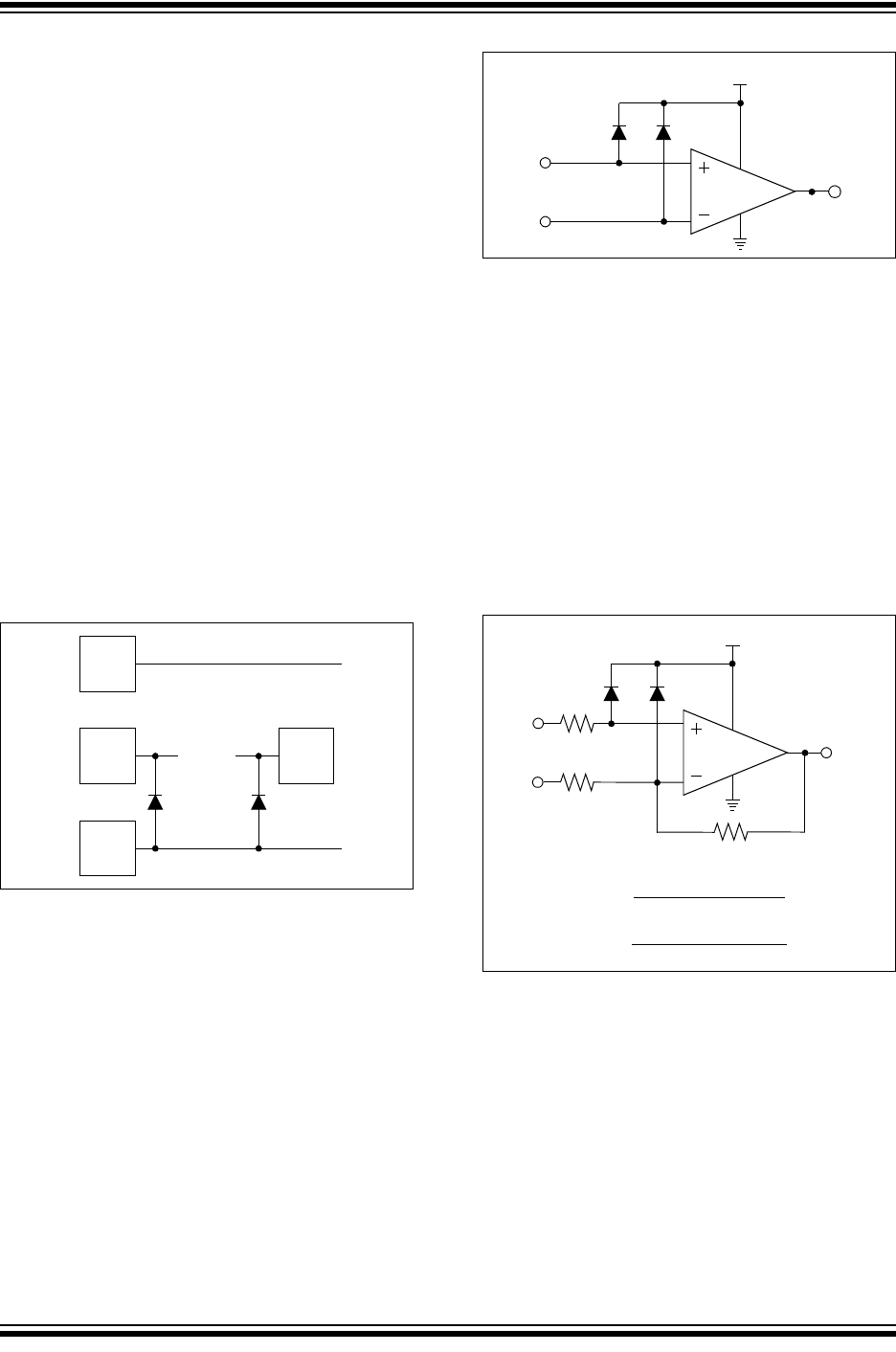
In some applications, it may be necessary to prevent
excessive voltages from reaching the op amp inputs;
Figure 4-2 shows one approach to protect these inputs.
FIGURE 4-2: Protecting the Analog
Inputs.
A significant amount of current can flow out of the
inputs when the Common mode voltage (V
CM
) is below
ground (V
SS
), as shown in Figure 2-34.
4.1.3 INPUT CURRENT LIMITS
In order to prevent damage and/or improper operation
of these amplifiers, the circuit must limit the currents
into the input pins (see Section 1.1 “Absolute
Maximum Ratings †”).
Figure 4-3 shows one approach to protect these inputs.
The R
1
and R
2
resistors limit the possible currents in or
out of the input pins (and the ESD diodes, D
1
and D
2
).
The diode currents will go through either V
DD
or V
SS
.
FIGURE 4-3: Protecting the Analog
Inputs.
Bond
Pad
Bond
Pad
Bond
Pad
V
DD
V
IN
+
V
SS
Input
Stage
Bond
Pad
V
IN
–
V
1
V
DD
D
1
V
2
D
2
MCP649X
V
OUT
V
1
R
1
V
DD
D
1
min (R
1
,R
2
) >
V
SS
–min(V
1
,V
2
)
2mA
min (R
1
,R
2
)>
max(V
1
,V
2
)–V
DD
2mA
V
2
R
2
D
2
R
3
V
OUT
MCP649X