
Datasheet


Table Of Contents
- Package Types
- Typical Application
- 1.0 Electrical Characteristics
- 2.0 Typical Performance Curves
- Figure 2-1: Input Offset Voltage
- Figure 2-2: Input Offset Voltage Drift
- Figure 2-3: Input Offset Voltage vs. Common Mode Input Voltage
- Figure 2-4: Input Offset Voltage vs. Common Mode Input Voltage
- Figure 2-5: Input Offset Voltage vs. Output Voltage
- Figure 2-6: Input Offset Voltage vs. Power Supply Voltage
- FIGURE 2-7: Input Noise Voltage Density vs. Frequency.
- FIGURE 2-8: Input Noise Voltage Density vs. Common Mode Input Voltage.
- FIGURE 2-9: CMRR, PSRR vs. Frequency.
- FIGURE 2-10: CMRR, PSRR vs. Ambient Temperature.
- FIGURE 2-11: Input Bias, Offset Currents vs. Ambient Temperature.
- FIGURE 2-12: Input Bias Current vs. Common Mode Input Voltage.
- FIGURE 2-13: Quiescent Current vs. Ambient Temperature.
- FIGURE 2-14: Quiescent Current vs. Common Mode Input Voltage.
- FIGURE 2-15: Quiescent Current vs. Common Mode Input Voltage.
- FIGURE 2-16: Quiescent Current vs. Power Supply Voltage.
- FIGURE 2-17: Open-Loop Gain, Phase vs. Frequency.
- FIGURE 2-18: DC Open-Loop Gain vs. Ambient Temperature.
- FIGURE 2-19: Gain Bandwidth Product, Phase Margin vs. Ambient Temperature.
- FIGURE 2-20: Gain Bandwidth Product, Phase Margin vs. Ambient Temperature.
- FIGURE 2-21: Output Short Circuit Current vs. Power Supply Voltage.
- FIGURE 2-22: Output Voltage Swing vs. Frequency.
- FIGURE 2-23: Output Voltage Headroom vs. Output Current.
- FIGURE 2-24: Output Voltage Headroom vs. Output Current.
- FIGURE 2-25: Output Voltage Headroom vs. Ambient Temperature.
- FIGURE 2-26: Output Voltage Headroom vs. Ambient Temperature.
- FIGURE 2-27: Slew Rate vs. Ambient Temperature.
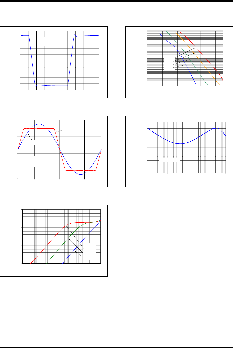
- FIGURE 2-28: Small Signal Non-Inverting Pulse Response.
- FIGURE 2-29: Small Signal Inverting Pulse Response.
- FIGURE 2-30: Large Signal Non-Inverting Pulse Response.
- FIGURE 2-31: Large Signal Inverting Pulse Response.
- FIGURE 2-32: The MCP6491/2/4 Shows No Phase Reversal.
- FIGURE 2-33: Closed Loop Output Impedance vs. Frequency.
- FIGURE 2-34: Measured Input Current vs. Input Voltage (below VSS).
- FIGURE 2-35: Channel-to-Channel Separation vs. Frequency (MCP6492/4 only).
- 3.0 Pin Descriptions
- 4.0 Application Information
- 5.0 Design Aids
- 6.0 Packaging Information
- Appendix A: Revision History
- Product Identification System
- Trademarks
- Worldwide Sales and Service
MCP6491/2/4
DS20002321C-page 12 2012-2013 Microchip Technology Inc.
Note: Unless otherwise indicated, T
A
=+25°C, V
DD
= +2.4V to +5.5V, V
SS
= GND, V
CM
=V
DD
/2, V
OUT
V
DD
/2,
V
L
=V
DD
/2, R
L
=10kto V
L
and C
L
=20pF.
FIGURE 2-31: Large Signal Inverting Pulse
Response.
FIGURE 2-32: The MCP6491/2/4 Shows
No Phase Reversal.
FIGURE 2-33: Closed Loop Output
Impedance vs. Frequency.
FIGURE 2-34: Measured Input Current vs.
Input Voltage (below V
SS
).
FIGURE 2-35: Channel-to-Channel
Separation vs. Frequency (MCP6492/4 only).
2.0
2.5
3.0
3.5
4.0
4.5
5.0
t
put Voltage (V)
V
DD
= 5 V
G = -1 V/V
0.0
0.5
1.0
1.5
Ou
t
Time (1 µs/div)
2
3
4
5
6
utput Voltages (V)
V
OUT
V
IN
-1
0
1
Input, O
Time (1 ms/div)
V
DD
= 5
V
G = +2 V/V
10
100
1000
o
sed Loop Output
Impedance (:)
G
N
:
101 V/V
1
1.0E+02 1.0E+03 1.0E+04 1.0E+05 1.0E+06 1.0E+07
Cl
o
Frequency (Hz)
101 V/V
11 V/V
1 V/V
100 1k 10k 100k 1M 10M
1.0E+04
1.0E+05
1.0E+06
1.0E+07
1.0E+08
1.0E+09
-I
IN
(pA)
1m
100µ
10µ
1µ
100n
10n
+125°C
+85°C
+25°C
40
°
C
1.0E+01
1.0E+02
1.0E+03
-1.0 -0.9 -0.8 -0.7 -0.6 -0.5 -0.4 -0.3 -0.2 -0.1 0.0
V
IN
(V)
1n
100p
10p
-
40
°
C
50
60
70
80
90
100
a
nnel to Channel
S
eparation (dB)
20
30
40
1.0E+02
1.0E+03
1.0E+04
1.0E+05
1.0E+06
Ch
a
S
Frequency (Hz)
100 1k 10k 100k 1M
Input Referred