MCP6491/2/4 7.5 MHz, Low-Input Bias Current Op Amps Features Description • Low-Input Bias Current - 150 pA (typical, TA = +125°C) • Low Quiescent Current - 530 µA/amplifier (typical) • Low-Input Offset Voltage - ±1.5 mV (maximum) • Supply Voltage Range: 2.4V to 5.5V • Rail-to-Rail Input/Output • Gain Bandwidth Product: 7.
MCP6491/2/4 Typical Application C2 R2 VOUT ID1 VDD – D1 Light MCP649X + Photodiode Amplifier DS20002321C-page 2 2012-2013 Microchip Technology Inc.
MCP6491/2/4 1.0 ELECTRICAL CHARACTERISTICS 1.1 Absolute Maximum Ratings † VDD – VSS ................................................................................................................................... ......................................................6.5V Current at Input Pins ................................................................................................................ ......................................................±2 mA Analog Inputs (VIN+, VIN-) (Note 1) ..
MCP6491/2/4 TABLE 1-1: DC ELECTRICAL SPECIFICATIONS (CONTINUED) Electrical Characteristics: Unless otherwise indicated, VDD = +2.4V to +5.5V, VSS = GND, TA = +25°C, VCM = VDD/2, VOUT VDD/2, VL = VDD/2 and RL = 10 kto VL. (Refer to Figure 1-1). Parameters Sym Min Typ Max Units Conditions VOH 2.380 2.396 — V VDD = 2.4V 0.5V input overdrive 5.480 5.493 — V VDD = 5.5V 0.5V input overdrive — 0.004 0.020 V VDD = 2.4V 0.5 V input overdrive — 0.007 0.020 V VDD = 5.5V 0.
MCP6491/2/4 1.3 Test Circuits The circuit used for most DC and AC tests is shown in Figure 1-1. This circuit can independently set VCM and VOUT (refer to Equation 1-1). Note that VCM is not the circuit’s common mode voltage ((VP + VM)/2), and that VOST includes VOS plus the effects (on the input offset error, VOST) of temperature, CMRR, PSRR and AOL. CF 6.
MCP6491/2/4 NOTES: DS20002321C-page 6 2012-2013 Microchip Technology Inc.
MCP6491/2/4 2.0 TYPICAL PERFORMANCE CURVES Note: The graphs and tables provided following this note are a statistical summary based on a limited number of samples and are provided for informational purposes only. The performance characteristics listed herein are not tested or guaranteed. In some graphs or tables, the data presented may be outside the specified operating range (e.g., outside specified power supply range) and therefore outside the warranted range.
MCP6491/2/4 Note: Unless otherwise indicated, TA = +25°C, VDD = +2.4V to +5.5V, VSS = GND, VCM = VDD/2, VOUT VDD/2, VL = VDD/2, RL = 10 kto VL and CL = 20 pF. 105 100 CMRR, PSRR (dB) 100 90 85 80 CMRR @ VDD = 5.5V @ VDD = 2.4V 75 70 65 10 0.1 1.E+0 1 1.E+1 10 1.E+2 100 1.E+3 1k 1.E+4 10k 1.E+5 100k 1.E+6 1M 1.E-1 Frequency (Hz) FIGURE 2-7: vs. Frequency. Input Noise Voltage Density -50 -25 0 FIGURE 2-10: Temperature. 100 125 CMRR, PSRR vs.
MCP6491/2/4 Note: Unless otherwise indicated, TA = +25°C, VDD = +2.4V to +5.5V, VSS = GND, VCM = VDD/2, VOUT VDD/2, VL = VDD/2, RL = 10 kto VL and CL = 20 pF. 700 575 VDD = 5.5V 550 525 VDD = 2.4V 500 475 600 Quiescent Current Q (µA/Amplifier) 500 300 200 VCM = VDD/4 100 VCM = VDD/4 6.5 FIGURE 2-16: Quiescent Current vs. Power Supply Voltage. Ope en-Loop Gain (dB) 650 600 550 500 450 VDD = 2.4V 350 -0.5 -0.3 -0.1 0.1 0.3 0.5 0.7 0.9 1.1 1.3 1.5 1.7 1.9 2.1 2.3 2.5 2.7 2.
MCP6491/2/4 70 12 60 10 50 Phase Margin 8 40 6 30 Gain Bandwidth Product 4 20 VDD = 2.4V 2 10 10 0 0 -25 0 25 50 75 100 Ambient Temperature (°C) 12 60 10 50 Phase Margin 8 40 6 30 Gain Bandwidth Product 4 20 VDD = 5.5V 2 Phase Margin (°) P Gain n Bandwidth Product (MHz) FIGURE 2-19: Gain Bandwidth Product, Phase Margin vs. Ambient Temperature. 70 10 0 -25 6.0 5.5 5.0 4.5 4.0 3.5 3.0 2.5 2.0 1.5 1.0 0.
MCP6491/2/4 7 Output Voltage (10 mV/div) Output Voltage Headroom (mV) Note: Unless otherwise indicated, TA = +25°C, VDD = +2.4V to +5.5V, VSS = GND, VCM = VDD/2, VOUT VDD/2, VL = VDD/2, RL = 10 kto VL and CL = 20 pF. 6 VDD - VOH 5 4 3 VOL - VSS 2 VDD = 2.4V 1 VDD = 5 V G = +1 V/V 0 -50 -25 0 25 50 75 Temperature (°C) 100 125 Time (0.2 µs/div) FIGURE 2-28: Pulse Response.
MCP6491/2/4 Note: Unless otherwise indicated, TA = +25°C, VDD = +2.4V to +5.5V, VSS = GND, VCM = VDD/2, VOUT VDD/2, VL = VDD/2, RL = 10 kto VL and CL = 20 pF. 1m 5.0 1.0E+09 4.5 1.0E+08 100µ VDD = 5 V G = -1 V/V 10µ 1.0E+07 -IIN (pA) 3.5 3.0 2.5 1µ 1.0E+06 1.0E+05 100n 2.0 1.0E+04 1.5 1.0E+03 10n 1n 1.0 100p 1.0E+02 0.5 1.0E+01 10p 0.0 -1.0 -0.9 -0.8 -0.7 -0.6 -0.5 -0.4 -0.3 -0.2 -0.1 0.0 VIN (V) Time (1 µs/div) FIGURE 2-31: Response.
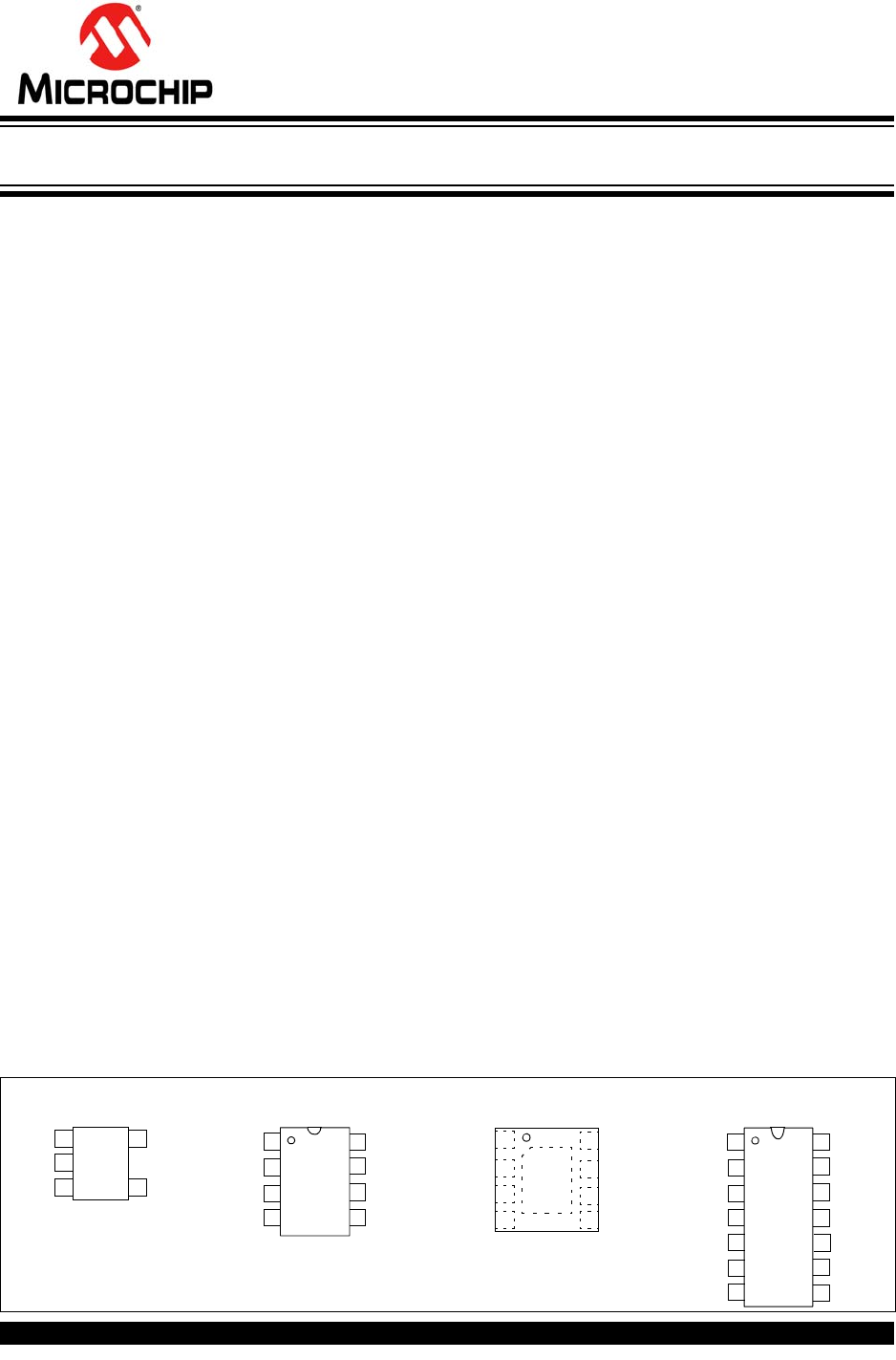
MCP6491/2/4 3.0 PIN DESCRIPTIONS Descriptions of the pins are listed in Table 3-1. TABLE 3-1: PIN FUNCTION TABLE MCP6491 MCP6492 MCP6494 Symbol Description 1 VOUT, VOUTA Analog Output (op amp A) 2 VIN–, VINA– Inverting Input (op amp A) Non-inverting Input (op amp A) SC70, SOT-23 SOIC, MSOP 2x3 TDFN SOIC, TSSOP 1 1 1 4 2 2 3.
MCP6491/2/4 NOTES: DS20002321C-page 14 2012-2013 Microchip Technology Inc.
MCP6491/2/4 4.0 APPLICATION INFORMATION The MCP6491/2/4 family of op amps is manufactured using Microchip’s state-of-the-art CMOS process and is specifically designed for low-power, high-precision applications. 4.1 VDD D1 D2 V1 VOUT Inputs 4.1.1 MCP649X V2 PHASE REVERSAL The MCP6491/2/4 op amps are designed to prevent phase reversal when the input pins exceed the supply voltages. Figure 2-32 shows the input voltage exceeding the supply voltage without any phase reversal. 4.1.
MCP6491/2/4 4.1.4 NORMAL OPERATION The inputs of the MCP6491/2/4 op amps use two differential input stages in parallel. One operates at a low Common mode input voltage (VCM), while the other operates at a high VCM. With this topology, the device operates with a VCM up to 0.3V above VDD and 0.3V below VSS (refer to Figures 2-3 and 2-4). The input offset voltage is measured at VCM = VSS – 0.3V and VDD + 0.3V to ensure proper operation. The transition between the input stages occurs when VCM is near VDD – 1.
MCP6491/2/4 4.5 Unused Op Amps 4.6 An unused op amp in a quad package (MCP6494) should be configured as shown in Figure 4-6. These circuits prevent the output from toggling and causing crosstalk. Circuit A sets the op amp at its minimum noise gain. The resistor divider produces any desired reference voltage within the output voltage range of the op amp, and the op amp buffers that reference voltage.
MCP6491/2/4 4.7 4.7.1 4.7.2 Application Circuits PHOTO DETECTION The MCP6491/2/4 op amps can be used to easily convert the signal from a sensor that produces an output current (such as a photo diode) into a voltage (a transimpedance amplifier). This is implemented with a single resistor (R2) in the feedback loop of the amplifiers shown in Figure 4-8 and Figure 4-9. The optional capacitor (C2) sometimes provides stability for these circuits.
MCP6491/2/4 4.7.3 PH ELECTRODE AMPLIFIER The MCP6491/2/4 op amps can be used for sensing applications where the sensor has high output impedance, such as a pH electrode sensor; its output impedance is in the range of 1 M to 1G. The key op amp specifications for these kinds of applications are low-input bias current and high-input impedance. A typical sensing circuit is shown in Figure 4-12, it is implemented with a non-inverting amplifier which has a gain of 1+R2/R1.
MCP6491/2/4 NOTES: DS20002321C-page 20 2012-2013 Microchip Technology Inc.
MCP6491/2/4 5.0 DESIGN AIDS Microchip Technology Inc. provides the basic design tools needed for the MCP6491/2/4 family of op amps. 5.1 SPICE Macro Model The latest SPICE macro model for the MCP6491/2/4 op amps is available on the Microchip web site at www.microchip.com. The model was written and tested in PSpice, owned by Orcad (Cadence®). For other simulators, translation may be required. The model covers a wide aspect of the op amp’s electrical specifications.
MCP6491/2/4 NOTES: DS20002321C-page 22 2012-2013 Microchip Technology Inc.
MCP6491/2/4 6.0 PACKAGING INFORMATION 6.1 Package Marking Information Example 5-Lead SOT-23 (MCP6491 only) Part Number MCP6491T-E/OT Code 3GNN 5-Lead SC-70 (MCP6491 only) Part Number MCP6491T-E/LTY 8-Lead MSOP (3x3 mm) (MCP6492 only) 3G25 Example Code DR25 DRNN Example 6492E 320256 8-Lead SOIC (3.90 mm) (MCP6492 only) Example MCP6492 E/SN1320 256 Legend: XX...
MCP6491/2/4 8-Lead TDFN (2x3x0.75 mm) (MCP6492 only) Example Part Number Code MCP6492T-E/MNY ABN 14-Lead SOIC (3.90 mm) (MCP6494 only) ABN 320 25 Example MCP6494 E/SL 1320256 14-Lead TSSOP (4.4 mm) (MCP6494 only) XXXXXXXX YYWW NNN DS20002321C-page 24 Example 6494E/ST 1320 256 2012-2013 Microchip Technology Inc.
MCP6491/2/4 5-Lead Plastic Small Outine Transistor (LTY) [SC70] Note: For the most current package drawings, please see the Microchip Packaging Specification located at http://www.microchip.com/packaging D b 3 1 2 E1 E 4 5 e A e A2 c A1 L ) + - 0 1 *++* % , *- -. - / ! 1 .' 3 4 5 1 6 % 6 4 5 5 2! " # .
MCP6491/2/4 5-Lead Plastic Small Outine Transistor (LTY) [SC70] Note: For the most current package drawings, please see the Microchip Packaging Specification located at http://www.microchip.com/packaging DS20002321C-page 26 2012-2013 Microchip Technology Inc.
MCP6491/2/4 9 6 ( < $==((( = 6 1 6 b N E E1 3 2 1 e e1 D A2 A c φ A1 L L1 ) + - 0 1 + 1 . + 1 *++* % , *- -. - ! ;! " # / ; " # .' 3 ; 5 1 6 % 6 4; 5 8 5 ! .
MCP6491/2/4 Note: For the most current package drawings, please see the Microchip Packaging Specification located at http://www.microchip.com/packaging DS20002321C-page 28 2012-2013 Microchip Technology Inc.
MCP6491/2/4 Note: For the most current package drawings, please see the Microchip Packaging Specification located at http://www.microchip.com/packaging 2012-2013 Microchip Technology Inc.
MCP6491/2/4 Note: For the most current package drawings, please see the Microchip Packaging Specification located at http://www.microchip.com/packaging DS20002321C-page 30 2012-2013 Microchip Technology Inc.
MCP6491/2/4 Note: For the most current package drawings, please see the Microchip Packaging Specification located at http://www.microchip.com/packaging 2012-2013 Microchip Technology Inc.
MCP6491/2/4 Note: For the most current package drawings, please see the Microchip Packaging Specification located at http://www.microchip.com/packaging DS20002321C-page 32 2012-2013 Microchip Technology Inc.
MCP6491/2/4 Note: For the most current package drawings, please see the Microchip Packaging Specification located at http://www.microchip.com/packaging 2012-2013 Microchip Technology Inc.
MCP6491/2/4 !" #$% & ' () 9 6 ( < $==((( = 6 DS20002321C-page 34 1 6 2012-2013 Microchip Technology Inc.
MCP6491/2/4 Note: For the most current package drawings, please see the Microchip Packaging Specification located at http://www.microchip.com/packaging 2012-2013 Microchip Technology Inc.
MCP6491/2/4 Note: For the most current package drawings, please see the Microchip Packaging Specification located at http://www.microchip.com/packaging DS20002321C-page 36 2012-2013 Microchip Technology Inc.
MCP6491/2/4 * + " , - . 9 6 ( < $==((( = 6 2012-2013 Microchip Technology Inc.
MCP6491/2/4 Note: For the most current package drawings, please see the Microchip Packaging Specification located at http://www.microchip.com/packaging DS20002321C-page 38 2012-2013 Microchip Technology Inc.
MCP6491/2/4 Note: For the most current package drawings, please see the Microchip Packaging Specification located at http://www.microchip.com/packaging 2012-2013 Microchip Technology Inc.
MCP6491/2/4 9 6 ( < $==((( = 6 DS20002321C-page 40 1 6 2012-2013 Microchip Technology Inc.
MCP6491/2/4 Note: For the most current package drawings, please see the Microchip Packaging Specification located at http://www.microchip.com/packaging 2012-2013 Microchip Technology Inc.
MCP6491/2/4 Note: For the most current package drawings, please see the Microchip Packaging Specification located at http://www.microchip.com/packaging DS20002321C-page 42 2012-2013 Microchip Technology Inc.
MCP6491/2/4 Note: For the most current package drawings, please see the Microchip Packaging Specification located at http://www.microchip.com/packaging 2012-2013 Microchip Technology Inc.
MCP6491/2/4 NOTES: DS20002321C-page 44 2012-2013 Microchip Technology Inc.
MCP6491/2/4 APPENDIX A: REVISION HISTORY Revision C (June 2013) The following is the list of modifications: 1. 2. 3. 4. 5. 6. 7. 8. Added new devices to the family (MCP6492 and MCP6494) and related information throughout the document. Updated thermal package resistance information in Table 1-3. Added Figure 2-35 in Section 2.0, Typical Performance Curves. Updated Section 3.0, Pin Descriptions. Added new Section 4.5, Unused Op Amps. Updated the list of reference documents in Section 5.
MCP6491/2/4 NOTES: DS20002321C-page 46 2012-2013 Microchip Technology Inc.
MCP6491/2/4 PRODUCT IDENTIFICATION SYSTEM To order or obtain information, e.g., on pricing or delivery, refer to the factory or the listed sales office. PART NO.
MCP6491/2/4 NOTES: DS20002321C-page 48 2012-2013 Microchip Technology Inc.
Note the following details of the code protection feature on Microchip devices: • Microchip products meet the specification contained in their particular Microchip Data Sheet. • Microchip believes that its family of products is one of the most secure families of its kind on the market today, when used in the intended manner and under normal conditions. • There are dishonest and possibly illegal methods used to breach the code protection feature.
Worldwide Sales and Service AMERICAS ASIA/PACIFIC ASIA/PACIFIC EUROPE Corporate Office 2355 West Chandler Blvd. Chandler, AZ 85224-6199 Tel: 480-792-7200 Fax: 480-792-7277 Technical Support: http://www.microchip.com/ support Web Address: www.microchip.