MCP616/7/8/9 2.3V to 5.5V Micropower Bi-CMOS Op Amps Features Description • • • • • • • • • • • The MCP616/7/8/9 family of operational amplifiers (op amps) from Microchip Technology Inc. are capable of precision, low-power, single-supply operation. These op amps are unity-gain stable, have low input offset voltage (±150 µV, maximum), rail-to-rail output swing and low input offset current (0.3 nA, typical). These features make this family of op amps well suited for battery-powered applications.
MCP616/7/8/9 NOTES: DS21613C-page 2 © 2008 Microchip Technology Inc.
MCP616/7/8/9 VDD – VSS ........................................................................7.0V † Notice: Stresses above those listed under “Absolute Maximum Ratings” may cause permanent damage to the device. This is a stress rating only and functional operation of the device at those or any other conditions above those indicated in the operational listings of this specification is not implied. Exposure to maximum rating conditions for extended periods may affect device reliability.
MCP616/7/8/9 AC ELECTRICAL CHARACTERISTICS Electrical Specifications: Unless otherwise indicated, VDD = +2.3V to +5.5V, VSS = GND, TA = 25°C, VCM = VDD/2, VOUT ≈ VDD/2, RL = 100 kΩ to VDD/2 and CL = 60 pF. Parameters Sym Min Typ Max Units kHz Conditions AC Response Gain Bandwidth Product GBWP — 190 — Phase Margin PM — 57 — ° Slew Rate SR — 0.08 — V/µs G = +1V/V Noise Input Noise Voltage Eni — 2.2 — µVP-P Input Noise Voltage Density eni — 32 — nV/√Hz f = 1 kHz f = 0.
MCP616/7/8/9 TEMPERATURE CHARACTERISTICS Electrical Specifications: Unless otherwise indicated, VDD = +2.3V to +5.5V and VSS = GND. Parameters Sym Min Typ Max Units Specified Temperature Range TA -40 — +85 °C Operating Temperature Range TA -40 — +125 °C Storage Temperature Range TA -65 — +150 °C Thermal Resistance, 8L-MSOP θJA — 211 — °C/W Thermal Resistance, 8L-PDIP θJA — 89.3 — °C/W Thermal Resistance, 8L-SOIC θJA — 149.
MCP616/7/8/9 NOTES: DS21613C-page 6 © 2008 Microchip Technology Inc.
MCP616/7/8/9 2.0 TYPICAL PERFORMANCE CURVES Note: The graphs and tables provided following this note are a statistical summary based on a limited number of samples and are provided for informational purposes only. The performance characteristics listed herein are not tested or guaranteed. In some graphs or tables, the data presented may be outside the specified operating range (e.g., outside specified power supply range) and therefore outside the warranted range.
MCP616/7/8/9 Note: Unless otherwise indicated, VDD = +2.3V to +5.5V, VSS = GND, TA = 25°C, VCM = VDD/2, VOUT ≈ VDD/2, RL = 100 kΩ to VDD/2 and CL = 60 pF. Input Bias Current (nA) Input Offset Voltage (µV) VDD = 5.5V Representative Part 100 VDD = 5.5V 50 0 VDD = 2.3V -50 -100 -150 -5 0.8 IOS -10 -15 0.4 IB -20 -25 0 25 50 75 100 -50 Ambient Temperature (°C) 0.2 115 VDD = 5.5V VDD = 2.
MCP616/7/8/9 100 0.30 0.25 0.20 0.15 0.10 0.05 0.00 -0.05 -0.10 -0.15 -0.20 -0.25 -0.30 IOS IB Common Mode Input Voltage (V) FIGURE 2-17: Input Offset Voltage vs. Common Mode Input Voltage. 5.5 5.0 4.5 4.0 3.5 3.0 2.5 1.5 VDD = 5.5V 1.0 100 Slew Rate vs. Ambient TA = +85°C TA = +25°C TA = -40°C 0.5 30 25 20 15 10 5 0 -5 -10 -15 -20 -25 -30 0.0 Input Bias Current (nA) FIGURE 2-14: Temperature.
MCP616/7/8/9 Note: Unless otherwise indicated, VDD = +2.3V to +5.5V, VSS = GND, TA = 25°C, VCM = VDD/2, VOUT ≈ VDD/2, RL = 100 kΩ to VDD/2 and CL = 60 pF. Output Voltage Headroom (mV) Quiescent Current (µA/Amplifier) 25 20 15 10 TA = +85°C TA = +25°C TA = -40°C 5 0 1,000 VDD = 2.3V 100 VDD – VOH 10 VOL – VSS 1 10µ 0.01 0.0 0.5 1.0 1.5 2.0 2.5 3.0 3.5 4.0 4.5 5.0 5.5 Power Supply Voltage (V) 125 DC Open-Loop Gain (dB) 125 120 VDD = 5.5V 110 VDD = 2.3V 95 90 100 0.
MCP616/7/8/9 0 120 -30 100 -60 Phase 80 -90 60 -120 40 -150 Gain 20 -180 0 -210 CMRR, PSRR (dB) 140 Open-Loop Phase (°) Open-Loop Gain (dB) Note: Unless otherwise indicated, VDD = +2.3V to +5.5V, VSS = GND, TA = 25°C, VCM = VDD/2, VOUT ≈ VDD/2, RL = 100 kΩ to VDD/2 and CL = 60 pF. -20 -240 0.01 1.E0.1 1.E+ 1 1.E+ 10 1.E+ 100 1.E+ 1k 1.E+ 10k 100k 1M 1.E1.E+ 1.E+ 02 01 00 Frequency 01 02 03 (Hz) 04 05 06 Open-Loop Gain, Phase vs.
MCP616/7/8/9 Note: Unless otherwise indicated, VDD = +2.3V to +5.5V, VSS = GND, TA = 25°C, VCM = VDD/2, VOUT ≈ VDD/2, RL = 100 kΩ to VDD/2 and CL = 60 pF. 5.0 Gain = +1 VDD = 5.0V 4 3 2 1 Gain = -1 VDD = 5.0V 4.5 Output Voltage (V) Output Voltage (V) 5 4.0 3.5 3.0 2.5 2.0 1.5 1.0 0.5 0 0.0 Time (50 µs/div) Time (50 µs/div) 5.0 10 4.5 5 4.0 3.5 3.0 CS VDD = 5.0V Gain = +1 V/V RL = 1 k to VSS 0 -5 -10 VOUT 2.5 2.0 1.5 1.0 -15 -20 Output High-Z Output On Output High-Z 0.
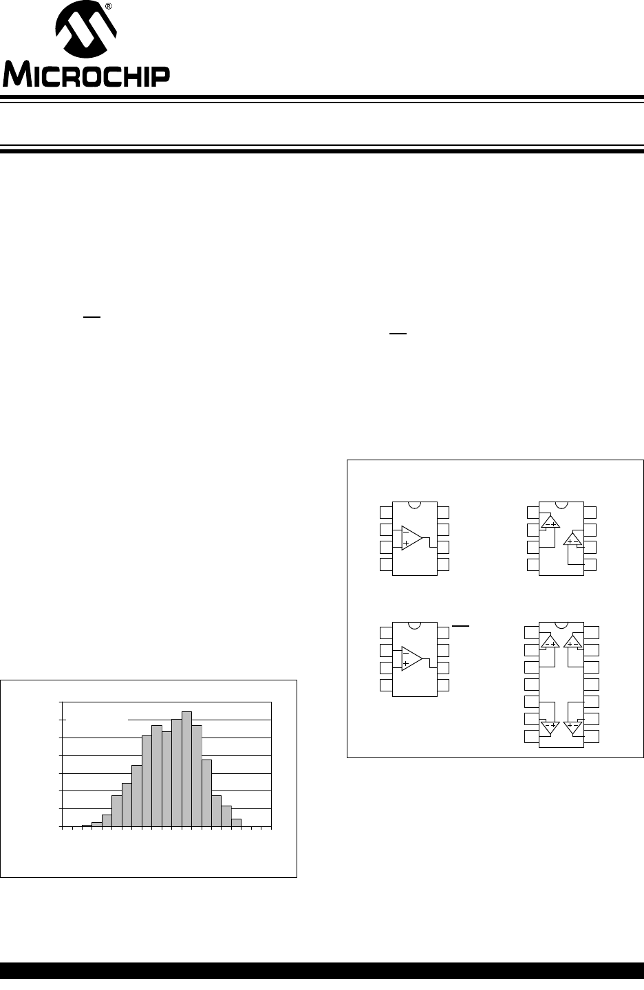
MCP616/7/8/9 3.0 PIN DESCRIPTIONS Descriptions of the pins are listed in Table 3-1.
MCP616/7/8/9 NOTES: DS21613C-page 14 © 2008 Microchip Technology Inc.
MCP616/7/8/9 4.0 APPLICATIONS INFORMATION The MCP616/7/8/9 family of op amps is manufactured using Microchip’s state-of-the-art CMOS process, which includes PNP transistors. These op amps are unity-gain stable and suitable for a wide range of general purpose applications. 4.1 Rail-to-Rail Inputs 4.1.1 VDD D1 V1 R1 R2 PHASE REVERSAL INPUT VOLTAGE AND CURRENT LIMITS The ESD protection on the inputs can be depicted as shown in Figure 4-1.
MCP616/7/8/9 EQUATION 4-1: R1 R2 GN = 1 + R2 ⁄ R1 V1 VOOS = GN [VOS + IB ((R1 ||R2) – REQ) C3 R3 – IOS ((R1 ||R2 ) + REQ ) / 2] MCP61X VCM = VEQ – (IB + IOS /2) REQ VOUT VOUT = VEQ (GN ) – V1 (GN – 1) + VOOS V2 Where: R4 R5 FIGURE 4-3: Example Circuit for Calculating DC Offset.
MCP616/7/8/9 4.4 Capacitive Loads 4.5 Driving large capacitive loads can cause stability problems for voltage feedback op amps. As the load capacitance increases, the feedback loop’s phase margin decreases and the closed-loop bandwidth is reduced. This produces gain peaking in the frequency response, with overshoot and ringing in the step response. A unity-gain buffer (G = +1) is the most sensitive to capacitive loads, though all gains show the same general behavior.
MCP616/7/8/9 4.8 PCB Surface Leakage 4.9 In applications where low input bias current is critical, Printed Circuit Board (PCB) surface leakage effects need to be considered. Surface leakage is caused by humidity, dust or other contamination on the board. Under low humidity conditions, a typical resistance between nearby traces is 1012Ω. A 5V difference would cause 5 pA of current to flow, which is greater than the MCP616/7/8/9 family’s bias current at 25°C (1 pA, typical).
MCP616/7/8/9 4.9.3 THREE OP AMP INSTRUMENTATION AMPLIFIER A classic, three-op amp instrumentation amplifier is illustrated in Figure 4-11. The two-input op amps provide differential signal gain and a common mode gain of +1. The output op amp is a difference amplifier, which converts its input signal from differential to a single-ended output; it rejects common mode signals at its input. The gain of this circuit is simply adjusted with one resistor (RG).
MCP616/7/8/9 NOTES: DS21613C-page 20 © 2008 Microchip Technology Inc.
MCP616/7/8/9 5.0 DESIGN AIDS Microchip provides the basic design tools needed for the MCP616/7/8/9 family of op amps. 5.1 SPICE Macro Model The latest SPICE macro model for the MCP616/7/8/9 op amps is available on the Microchip web site at www.microchip.com. This model is intended to be an initial design tool that works well in the op amp’s linear region of operation over the temperature range. See the model file for information on its capabilities.
MCP616/7/8/9 NOTES: DS21613C-page 22 © 2008 Microchip Technology Inc.
MCP616/7/8/9 6.0 PACKAGING INFORMATION 6.1 Package Marking Information Example: 8-Lead MSOP XXXXXX 616I YWWNNN 812256 8-Lead PDIP (300 mil) XXXXXXXX XXXXXNNN YYWW MCP616 I/P256 0812 8-Lead SOIC (150 mil) XXXXXXXX XXXXYYWW NNN Legend: XX...
MCP616/7/8/9 Package Marking Information (Continued) 14-Lead PDIP (300 mil) (MCP619) XXXXXXXXXXXXXX XXXXXXXXXXXXXX YYWWNNN 14-Lead SOIC (150 mil) (MCP619) Examples: MCP619-I/P XXXXXXXXXXXXXX 0812256 Examples: XXXXXXXXXX XXXXXXXXXX YYWWNNN 14-Lead TSSOP (MCP619) XXXXXXXX YYWW NNN DS21613C-page 24 OR MCP619 e3 I/P^^ 0812256 MCP619ISL XXXXXXXXXX 0812256 OR MCP619 e3 I/SL ^^ 0812256 Example: 619IST 0812 256 © 2008 Microchip Technology Inc.
MCP616/7/8/9 1 % & % ! % 2 " ) ' % 2 $ % % " % %% 033))) & &3 2 D N E E1 NOTE 1 1 2 e b A2 A c φ L L1 A1 4 % & 5 & % 6!&( $ 55 * * 6 6 67 8 9 % 7 ; % < < + 9+ + < + " " 2 2 % " $$ :+ . / 7 = "% * " " 2 = "% * , .
MCP616/7/8/9 ! "## $ % 1 % & % ! % 2 " ) ' % 2 $ % % " % %% 033))) & &3 2 N NOTE 1 E1 1 3 2 D E A2 A L A1 c e eB b1 b 4 % & 5 & % 6!&( $ 6/;* 6 6 % 8 9 % % 67 . / < < + , + .
MCP616/7/8/9 ! &' "()# $ % * 1 % & % ! % 2 " ) ' % 2 $ % % " % %% 033))) & &3 2 D e N E E1 NOTE 1 1 2 3 α h b h A2 A c φ L A1 L1 4 % & 5 & % 6!&( $ β 55 * * 6 6 67 8 9 % 7 ; % < < + < < < + " " 2 2 % " $$ ? . / + 7 = "% * " " 2 = "% * , .
MCP616/7/8/9 ! &' "()# $ % * 1 % & % ! % 2 " ) ' % 2 $ % % " % %% 033))) & &3 2 DS21613C-page 28 © 2008 Microchip Technology Inc.
MCP616/7/8/9 +, ! "## $ % 1 % & % ! % 2 " ) ' % 2 $ % % " % %% 033))) & &3 2 N NOTE 1 E1 1 3 2 D E A2 A L A1 c b1 b e eB 4 % & 5 & % 6!&( $ 6/;* 6 6 % 8 % % 67 . / < < + , + .
MCP616/7/8/9 +, ! &' "()# $ % * 1 % & % ! % 2 " ) ' % 2 $ % % " % %% 033))) & &3 2 D N E E1 NOTE 1 1 2 3 e h b A2 A α h c φ L A1 β L1 4 % & 5 & % 6!&( $ 55 * * 6 6 67 8 % 7 ; % < < + < < < + " " 2 2 % " $$ ? . / 7 = "% * " " 2 = "% * , .
MCP616/7/8/9 1 % & % ! % 2 " ) ' % 2 $ % % " % %% 033))) & &3 2 © 2008 Microchip Technology Inc.
MCP616/7/8/9 +, -. . - ! ,(, $ % - 1 % & % ! % 2 " ) ' % 2 $ % % " % %% 033))) & &3 2 D N E E1 NOTE 1 1 2 e b A2 A c A1 φ L L1 4 % & 5 & % 6!&( $ 55 * * 6 6 67 8 % 7 ; % < < 9 + + < + " " 2 2 % " $$ :+ .
MCP616/7/8/9 APPENDIX A: REVISION HISTORY Revision C (October 2008) The following is the list of modifications: 1. 2. 3. 4. 5. 6. Added Section 1.1 “Test Circuits”. Added Figure 2-36. Added Section 4.1.1 “Phase Reversal”, Section 4.1.2 “Input Voltage and Current Limits”, and Section 4.1.3 “Normal Operation”. Updated Figure 4-7. Updated Section 5.0 “Design Aids”. Updated Section 6.0 “Packaging Information” Revision B (April 2005) The following is the list of modifications: 1. 2. 3. 4. 5. 6. 7.
MCP616/7/8/9 NOTES: DS21613C-page 30 © 2008 Microchip Technology Inc.
MCP616/7/8/9 PRODUCT IDENTIFICATION SYSTEM To order or obtain information, e.g., on pricing or delivery, refer to the factory or the listed sales office. PART NO.
MCP616/7/8/9 NOTES: DS21613C-page 32 © 2008 Microchip Technology Inc.
Note the following details of the code protection feature on Microchip devices: • Microchip products meet the specification contained in their particular Microchip Data Sheet. • Microchip believes that its family of products is one of the most secure families of its kind on the market today, when used in the intended manner and under normal conditions. • There are dishonest and possibly illegal methods used to breach the code protection feature.
WORLDWIDE SALES AND SERVICE AMERICAS ASIA/PACIFIC ASIA/PACIFIC EUROPE Corporate Office 2355 West Chandler Blvd. Chandler, AZ 85224-6199 Tel: 480-792-7200 Fax: 480-792-7277 Technical Support: http://support.microchip.com Web Address: www.microchip.