
User manual
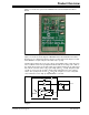
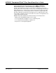
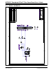
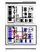
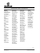
Table Of Contents
Product Overview
© 2008 Microchip Technology Inc. DS51763A-page 7
Figure 1-3 shows the top view of the MCP6031 Photodiode PICtail™ Plus Demo
Board.
FIGURE 1-3: Top view of MCP6031 Photodiode PICtail™ Plus Demo Board
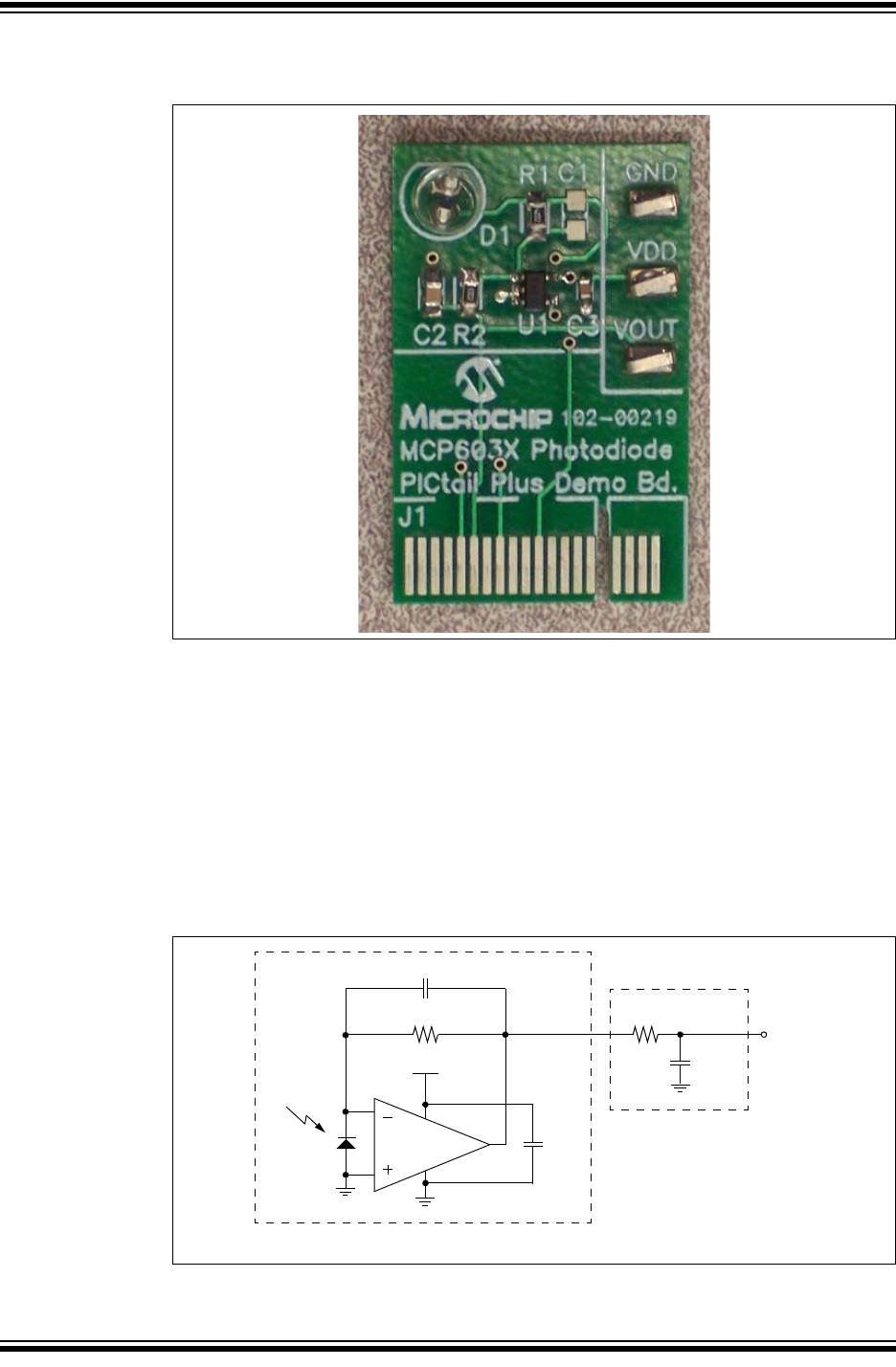
Figure 1-4 shows the circuit diagram of MCP6031 Photodiode PICtail™ Plus Demo
Board. C
1
is for compensation purpose and no need for the board. It may be needed
when MCP6031 is replaced by the other Microchip’s op amp.
The DC output voltage due to the source photo-current will be V
OUT
= I
S
R
1
, where R
1
is the feedback resistor. The op amp will contribute a DC offset voltage, V
OS
+ I
B
R
1
, to
the output, where V
OS
is the op amp’s input offset voltage and I
B
is the op amp’s input
bias current. Select the value of R
1
to give a high gain to I
S
. Usually, this gain is high
enough to use most of the op amp’s output voltage swing when I
S
is at its extreme
values. The op amp needs to have V
OS
and I
B
low enough to not cause a large DC
offset. That is the reason why op amp MCP6031 is selected.
.
FIGURE 1-4: MCP6031 Photodiode PICtail™ Plus Demo Board Circuit
Diagram.
33 nF
10 kΩ
C
1
Transimpedance Amplifier
Low-Pass Filter
unpopulated
U1
D
1
R
1
42.2 kΩ
R
2
C
2
C3
+3.3V
V
OUT
PNZ334
MCP6031
0.1 µF