
Datasheet


MCP4XXX Digital Potentiometer Daughter Board User’s Guide
DS51621A-page 16 © 2006 Microchip Technology Inc.
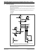
2.4 MCP4XXX DIGITAL POTENTIOMETER DAUGHTER BOARD DESCRIPTION
The MCP4XXX Digital Potentiometer Daughter Board PCB is designed to be flexible in
the type of device evaluation that can be implemented.
The following sections describe each element of this evaluation board in further detail.
2.4.1 Power and Ground
The MCP4XXX Digital Potentiometer Daughter Board receives its power over the J3
header connector. If the board is to be jumpered into an existing application, then the
board can have connection posts installed for the power (V
DD
) and ground (V
SS
), which
are located below device U2. The layout allows through-hole connection posts.
2.4.2 Connection Pads
The MCP4XXX Digital Potentiometer Daughter Board has pads for all the resistor net-
work signal. These are:
There are three pads for control signals that are also available:
• U1-CS0/U3-CS
•U2-CS1
•U3-UD
2.4.3 Passive Components (R1, R2, R3, R4, R5, R6, R7, R8, R9, R10,
R11, R12, R13, R14, R15 and R16)
The footprints for these components are present to allow flexibility in the use of fixed
resistors for the windowing of the U1-Pot0 (or U3-Pot) to better match your system
requirements.
U1-P0A
U1-P0W
U1-P0B
Socket U1 Potentiometer 0
U1-P01A
U1-P1W
U1-P1B
Socket U1 Potentiometer 1
U2-P0A
U2-P0W
U2-P0B
Socket U2 Potentiometer 0
U2-P01A
U2-P1W
U2-P1B
Socket U2 Potentiometer 1
U3-1A
U3-W
U3-B
Socket U3 Device only contains single
Potentiometer
Resistors
Used
Jumpers
Required
Device Configuration Comments
R1 & R3 — U2-Pot0 is windowed
R2 & R16 — U2-Pot1 is windowed
R1 & R2 JP1, JP5, JP9,
& JP10
U1-Pot0 is windowed
R1 & R16 — U2-Rheo0 Trims R1
U2-Rheo1 Trims R16
U1-Pot0 is windowed