
User manual

MCP4728 EVALUATION BOARD
USER’S GUIDE
© 2009 Microchip Technology Inc. DS51837A-page 43
Appendix C. MCP4728 Read/Write Commands
C.1 INTRODUCTION
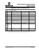
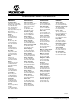
Table summarizes the write command types and their functions. The write command
is defined by using three write command type bits (C2, C1, C0) and two write function
bits (W1, W0). Writing and reading the I
2
C address bits are not demonstrated with the
PICKit Serial Analyzer. Please see the MCP4728 data sheet for more details on the
commands.
TABLE C-1: WRITE COMMAND TYPES
Command Field
Write
Function
Command Name Function
C2 C1 C0 W1 W0
Fast Mode Write
0 0 X Not Used Fast Write for DAC
Input Registers
This command writes to the DAC input registers sequentially
with limited configuration bits. The data is sent sequentially
from channels A to D. The input register is written at the
acknowledge clock pulse of the channel’s last input data byte.
EEPROM is not affected. (Note 1)
Write DAC Input Register and EEPROM
01000Multi-Write for DAC
Input Registers
This command writes to multiple DAC input registers, one DAC
input register at a time. The writing channel register is defined
by the DAC selection bits (DAC1, DAC0). EEPROM is not
affected. (Note 2)
1 0 Sequential Write for
DAC Input Regis-
ters and EEPROM
This command writes to both the DAC input registers and
EEPROM sequentially. The sequential writing is carried out
from a starting channel to channel D. The starting channel is
defined by the DAC selection bits (DAC1 and DAC0).
The input register is written at the acknowledge clock pulse of
the last input data byte of each register. However, the
EEPROM data is written altogether at the same time sequen-
tially at the end of the last byte. (Note 2),(Note 3)
1 1 Single Write for
DAC Input Register
and EEPROM
This command writes to a single selected DAC input register
and its EEPROM. Both the input register and EEPROM are
written at the acknowledge clock pulse of the last input data
byte. The writing channel is defined by the DAC selection bits
(DAC1 and DAC0). (Note 2),(Note 3)
Write I
2
C Address Bits (A2, A1, A0)
0 1 1 Not Used Write I
2
C Address
Bits
This command writes new I
2
C address bits (A2, A1, A0) to the
DAC input register and EEPROM.
Note 1: The analog output is updated when LDAC pin is (or changes to) “Low”. UDAC bit is not used for this
command.
2: The DAC output is updated when LDAC
pin or UDAC bit is “Low”.
3: The device starts writing to the EEPROM on the acknowledge clock pulse of the last channel. The device
does not execute any command until RDY/BSY
bit comes back to “High”.
4: The input and output registers are updated at the acknowledge clock pulse of the last byte. The update
does not require LDAC
pin or UDAC bit conditions. EEPROM is not affected.