
User manual

Quick Start Instructions
© 2009 Microchip Technology Inc. DS51837A-page 31
.
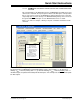
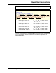
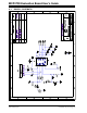
FIGURE 1-21: The contents of the Registers and EEPROM. The order of the
contents: Channel A Register and EEPROM, and Channel B Register and EEPROM,
and so on sequentially. See the Read Command and Device Output details in
MCP4728 Data Sheet.
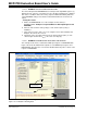
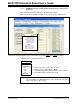
Note: In Figure 1-20, the script file called “MCP4728_Read” was created, saved
and executed.
DAC A Register
DAC A EEPROM
DAC B Register
DAC B EEPROM
DAC C EEPROM
DAC C Register
DAC D Register
DAC C EEPROM
Ch. A Register: C0-0F-FF: V
REF
= V
DD
, G
A
= x1, Data = FFFh
Ch. A EEPROM: C8-0F-FF: V
REF
= V
DD
, G
A
= x1, Data = FFFh
Ch. B Register: D0-0F-FF: V
REF
= V
DD
, G
A
= x1, Data = FFFh
Ch. B EEPROM: D8-0F-FF: V
REF
= V
DD
, G
A
= x1, Data = FFFh
Ch. C Register: E0-8F-FF: V
REF
= V
DD
, G
A
= x1, Data = FFFh
Ch. C EEPROM: E8-0F-FF: V
REF
= V
DD
, G
A
= x1, Data = FFFh
Ch. D Register: F0-90-FF: V
REF
= V
DD
, G
A
= x2, Data = 0FFh
Ch. D EEPROM: F8-90-FF: V
REF
= V
DD
, G
A
= x2, Data = 0FFh