
User manual


MCP4728 Evaluation Board User’s Guide
DS51837A-page 30 © 2009 Microchip Technology Inc.
1.3.2.14 EXAMPLE 7: TESTING EEPROM FEATURES
The device will upload the EEPROM data to both input and output DAC registers (a)
during power-up sequence or (b) when it receives the General Call Reset command.
One of these conditions makes the analog outputs available immediately with their
current EEPROM settings. Note that the Power-Down bit must be cleared for the
output.
• Testing Procedure:
a. Write to the EEPROM with one of the examples shown earlier (i.e.,
Section 1.3.2.12 “Example 6: Sequential Write for DAC Input Registers and
EEPROM”).
b. Measure and record the analog voltage of each channel (V
OUT
) using a
multimeter.
c. Turn-off the V
DD
of the device. If you are using the V
DD
from the PICkit Serial
Analyzer, disconnect JP1 connect.
d. Turn-back on the V
DD
again and measure the analog voltage (V
OUT
) of each
channel again. Confirm the V
OUT
is the same as in Step (b).
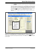
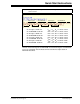
1.3.2.15 EXAMPLE 8: READING DAC REGISTERS AND EEPROM
This example shows how to read back the DAC input registers and EEPROM data.
Figure 1-20 shows the PICkit Serial script file to read all DAC input registers and
EEPROM data. Once this file is executed, the PC GUI will show you the contents of the
registers and EEPROM.
.
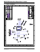
FIGURE 1-20: Reading the DAC Registers and its EEPROM with a Read Command. See
Figure 1-21 for Details in Reading Data.
18h = 24 (decimal):
Requesting 24 bytes.
Read Command
Reading Data