
User manual

Quick Start Instructions
© 2009 Microchip Technology Inc. DS51837A-page 29
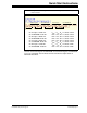
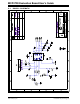
FIGURE 1-19: V
OUT
for Example 6: V
OUT
after Sequential Write Command.
V
OUT
V
REF
D
n
×
()
4096
------------------------------ -
G
x
=
Where:
V
REF
=V
DD
if external V
REF
is selected
= 2.048V if internal V
REF
is selected.
D
n
= Input code
LSB = V
REF
/4096
V
OUT
B
V
DD
4095
×
()
4096
--------------------------------- -
G
x
V
DD
4096 1–
4096
-------------------- -
⎝⎠
⎛⎞
V
DD
1
1
4096
----------- -–
⎝⎠
⎛⎞
V
DD
LSB–====
In Script file, V
REF
= V
DD
, Gain (G
X
) = 1, Dn for Channel B = 0FFF (hex) = 4095 (decimal)
(A) DAC A Output:
Note that Dn and Gain (Gx) must be selected with the following conditions:
V
OUT
V
REF
D
n
×
()
4096
------------------------------ -
G
x
V
DD
≤
=
(B) DAC B Output:
(C) DAC C Output:
(D) DAC D Output:
No change. Keep its output with previous settings.
In Script file, V
REF
= Internal, Gain (G
X
) = 1, Dn for Channel C = 0FFF (hex) = 4095 (decimal)
V
OUT
C
V
REF
4095
×
()
4096
------------------------------------
G
x
V
REF
4096 1–
4096
-------------------- -
⎝⎠
⎛⎞
V
REF
1
1
4096
----------- -–
⎝⎠
⎛⎞
V
REF
LSB–====
where V
REF
= internal = 2.048V, LSB =0.5 mV
In Script file, V
REF
= Internal, Gain = 2, Dn for Channel D = 00FF (hex) = 255 (decimal)
V
OUT
D
V
REF
255
×
4096
----------------------------
G
x
V
REF
255
4096
----------- -
⎝⎠
⎛⎞
2V
REF
0.06226()2() 0.255V====
= 2.0475
where V
REF
= internal = 2.048V