
User manual


MCP4728 Evaluation Board User’s Guide
DS51837A-page 6 © 2009 Microchip Technology Inc.
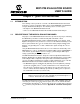
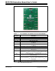
FIGURE 1-1: Front View of the MCP4728 Evaluation Board.
TABLE 1-1: TEST TERMINALS ON THE MCP4728 EVALUATION BOARD
Test
Terminals
Description
V
OUT
A DAC channel A output
V
OUT
B DAC channel B output
V
OUT
C DAC channel C output
V
OUT
D DAC channel D output
SCL This terminal is connected to the I
2
C SCL pin of the MCP4728.
(See Note 1).
SDA This terminal is connected to the I
2
C SDA pin of the MCP4728.
(See Note 1).
RDY/BUSY
This terminal is used to monitor the RDY/BUSY pin of the MCP4728 device.
LDAC
Access terminal to the LDAC pin of the MCP4728.
S1 Switch to change the logic input to the LDAC
input pin. It provides logic “low”
when pressed.
JP1 Jumper to select the V
DD
source to the MCP4728 Evaluation Board. If it is
connected, the V
DD
from the J1 connector is connected. If disconnected, it
selects the V
DD
source from VDD1 terminal.
JP2 Jumper to connect the LDAC pin to V
SS
. (You can disconnect this jumper
when S1 is used.)
VDD1 V
DD
monitoring or connection pin.
If the V
DD
is provided from J1 connector (PICkit Serial Analyzer), then this
test point monitors the V
DD
voltage. You can also connect a new V
DD
to this
test terminal.
GND Connected to common ground plane of the PC Board.
Note 1: This terminal is used to monitor the SCL or SDA signals. You can also provide the
SCL or SDA signals through these pins.