
Datasheet


© 2010 Microchip Technology Inc. DS22187E-page 55
MCP4728
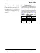
FIGURE 7-4: Sequential Write Command for Setting Test Points in Figure 7-3.
Expected Output Voltage at Each Channel:
V
OUT
AV
DD
D
n
4096
------------
V
DD
2048
4096
------------
V
DD
2
-----------
=
×
=
×
V()=
V
OUT
BV
DD
D
n
4096
------------V
DD
4095
4096
------------V
DD
LSB–()V()=
×
=
×
=
V
OUT
CV
REF
D
n
4096
------------G
x
2.048
2048
4096
------------ × 22.048V()=
×
=
×
=
V
OUT
DV
REF
D
n
4096
------------G
x
2.048
4095
4096
------------ × 24.096V()=
×
=
×
=
S11000000A01010000A00001000A00000000A
1st Byte
Channel A as
SelectingSequential Write
CommandDevice Addressing
Dn = 2
11
= 2048
UDAC
V
REF
ACK (MCP4728)
G
X
R/W
Update DAC A Input Register at this ACK pulse.
Starting Channel
00001111
A11111111A
ACK (MCP4728)
V
REF
G
X
Dn = 4095
10011000A00000000A
ACK (MCP4728)
V
REF
G
X
Dn = 2048
Update DAC B Input Register at this ACK pulse.
Update DAC C Input Register at this ACK pulse.
10011111A11111111A P
ACK (MCP4728)
V
REF
G
X
Dn = 4095
Update DAC D Input Register at this ACK pulse.
Stop
Start
for Writing