
Datasheet


© 2010 Microchip Technology Inc. DS22187E-page 5
MCP4728
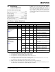
Analog Output (Output Amplifier)
Output Voltage Swing V
OUT
— FSR — V Note 7
Full Scale Range
(Note 7)
FSR — V
DD
—VV
REF
=V
DD
FSR = from 0.0V to V
DD
—V
REF
—VV
REF
= Internal, G
x
=1,
FSR = from 0.0 V to V
REF
—2*V
REF
—VV
REF
= Internal, G
x
=2,
FSR = from 0.0V to 2 * V
REF
Output Voltage
Settling Time
T
SETTLING
—6—µsNote 8
Analog Output Time Delay
from Power-Down Mode
Td
ExPD
—4.5— µsV
DD
=5V,
Note 4, Note 9
Time delay to settle to new
reference
(Note 4, Note 6)
Td
REF
— 26 — µs From External to Internal
Reference
— 44 — µs From Internal to External
Reference
Power Supply Rejection PSRR — -57 — dB V
DD
=5V±10%, V
REF
= Internal
Capacitive Load Stability C
L
— — 1000 pF R
L
=5kΩ
No oscillation, Note 4
Slew Rate SR — 0.55 — V/µs
Phase Margin p
M
— 66 — Degree
(°)
C
L
=400pF, R
L
= ∞
Short Circuit Current I
SC
—1524mA V
DD
=5V,
All V
OUT
Pins = Grounded.
Tested at room temperature.
Short Circuit Current
Duration
T
SC_DUR
— Infinite — hours Note 4
DC Output Impedance
(Note 4)
R
OUT
—1 —Ω Normal mode
—1—kΩ Power-Down mode 1
(PD1:PD0 = 0:1), V
OUT
to V
SS
—100— kΩ Power-Down mode 2
(PD1:PD0 = 1:0), V
OUT
to V
SS
—500— kΩ Power-Down mode 3
(PD1:PD0 = 1:1), V
OUT
to V
SS
ELECTRICAL CHARACTERISTICS (CONTINUED)
Electrical Specifications: Unless otherwise indicated, all parameters apply at V
DD
= +2.7V to 5.5V, V
SS
=0V,
R
L
=5kΩ, C
L
= 100 pF, G
X
=1, T
A
= -40°C to +125°C. Typical values are at +25°C, V
IH
=V
DD
, V
IL
=V
SS.
Parameter Symbol Min Typical Max Units Conditions
Note 1: All digital input pins (SDA, SCL, LDAC
) are tied to “High”, Output pins are unloaded, code = 0 x 000.
2: The power-up ramp rate measures the rise of V
DD
over time.
3: This parameter is ensured by design and not 100% tested.
4: This parameter is ensured by characterization and not 100% tested.
5: Test code range: 100 - 4000 codes, V
REF
= V
DD
, V
DD
= 5.5V.
6: Time delay to settle to a new reference when switching from external to internal reference or vice versa.
7: This parameter is indirectly tested by Offset and Gain error testing.
8: Within 1/2 LSB of the final value when code changes from 1/4 of to 3/4 of full scale.
9: This time delay is measured from the falling edge of ACK pulse in I
2
C command to the beginning of V
OUT
.
This time delay is not included in the output settling time specification.