
Datasheet


MCP4728
DS22187E-page 38 © 2010 Microchip Technology Inc.
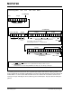
FIGURE 5-7: Fast Write Command: Write DAC Input Registers Sequentially from Channel A to D.
1st byte
DAC Input Register of Channel A
2nd Byte
R/W
Device Addressing
ACK (MCP4728)
(C2 C1) 3rd Byte
Update Channel A DAC Input Register at this ACK pulse.
Repeat Bytes
Start
Stop
Fast Write
Note 1: X is a don’t care bit. V
OUT
can be updated after the last byte’s ACK pulse is issued and by
bringing down the LDAC
pin to “Low”.
2nd Byte
ACK (MCP4728)
3rd Byte
Update Channel B DAC Input Register at this ACK pulse.
DAC Input Register of Channel B
S1100A2A1A00A 0 0 PD1 PD0 D11 D10 D9 D8 A D7D6D5D4D3D2D1D0 A
Command Type Bits: C2=0 C1=0 C0=X
Command
X X PD1 PD0 D11 D10 D9 D8
A D7D6D5D4D3D2D1D0 A
2nd Byte
ACK (MCP4728)
3rd Byte
Update Channel C DAC Input Register at this ACK pulse.
DAC Input Register of Channel C
X X PD1 PD0 D11 D10 D9 D8
A D7D6D5D4D3D2D1D0 A
2nd Byte
ACK (MCP4728)
3rd Byte
Update Channel D DAC Input Register at this ACK pulse.
DAC Input Register of Channel D
X X PD1 PD0 D11 D10 D9 D8
A D7D6D5D4D3D2D1D0 A
P