
Datasheet


© 2010 Microchip Technology Inc. DS22187E-page 33
MCP4728
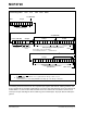
5.4.4 GENERAL CALL READ ADDRESS
BITS
This command is used to read the I
2
C address bits of
the device. If the second byte is “00001100” (0Ch), the
device will output its address bits stored in EEPROM
and register. This command uses the LDAC
pin to
select the device of interest to read on the I
2
C bus. The
LDAC
pin needs a logic transition from “High” to “Low”
during the negative pulse of the 8th clock of the second
byte, and stays “Low” until the end of the 3rd byte. The
maximum clock rate for this command is 400 kHz.
FIGURE 5-6: General Call Read I
2
C Address.
ACK
(MCP4728)
Restart
(General Call Address)
1st Byte
2nd Byte Address Bits
in
Address Bits
in Input
Note 3
(Notes 1, 2, 3)
LDAC
Pin
4th Byte
ACK (Master)
Start
3rd Byte
Note 3
ACK Clock
Clock Pulse
LDAC Pin
2nd Byte
3rd Byte
4th Byte
Note 2 (a)
ACK Clock
Note 2(b)
Stay “Low” until the end of the 3rd Byte
Note 2(b, c)
Restart Clock
(CLK Line)
Reading Address Bits
Reading Address Bits
Stop
6 7 8 9 Sr 1 2 3 4 5 6 7 8 9 1 2 3
Note 1: Clock Pulse and LDAC Transition Details.
2: LDAC
pin events at the 2nd and 3rd bytes.
a. Keep LDAC
pin “High” until the end of the positive pulse of the 8th clock of the 2nd byte.
b. LDAC
pin makes a transition from “High” to “Low” during the negative pulse of the 8th clock of the 2nd
byte (just before the rising edge of the 9th clock) and stays “Low” until the rising edge of clock 9 of the
3rd byte.
c. The MCP4728 device does not acknowledge the 3rd byte if the conditions (a) and (b) are not met.
3: LDAC
pin resumes its normal function after “Stop” bit.
S00000000A00001100A Sr1100XXX1AA2A1A0 1 A2A1A0 0 A P
Restart Byte
EEPROM
Register
Clock and LDAC Transition Details: