
Datasheet


© 2010 Microchip Technology Inc. DS22187E-page 3
MCP4728
1.0 ELECTRICAL
CHARACTERISTICS
Absolute Maximum Ratings†
V
DD
...................................................................................6.5V
All inputs and outputs w.r.t V
SS
................. -0.3V to V
DD
+0.3V
Current at Input Pins ....................................................±2 mA
Current at Supply Pins .............................................±110 mA
Current at Output Pins ...............................................±25 mA
Storage Temperature ...................................-65°C to +150°C
Ambient Temp. with Power Applied .............-55°C to +125°C
ESD protection on all pins ................ ≥ 4 kV HBM, ≥ 400V MM
Maximum Junction Temperature (T
J
) .........................+150°C
† Notice: Stresses above those listed under “Maximum
ratings” may cause permanent damage to the device. This is
a stress rating only and functional operation of the device at
these or any other conditions above those indicated in the
operation listings of this specification is not implied. Exposure
to maximum rating conditions for extended periods may affect
device reliability.
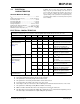
ELECTRICAL CHARACTERISTICS
Electrical Specifications: Unless otherwise indicated, all parameters apply at V
DD
= +2.7V to 5.5V, V
SS
=0V,
R
L
=5kΩ, C
L
= 100 pF, G
X
=1, T
A
= -40°C to +125°C. Typical values are at +25°C, V
IH
=V
DD
, V
IL
=V
SS.
Parameter Symbol Min Typical Max Units Conditions
Power Requirements
Operating Voltage V
DD
2.7 5.5 V
Supply Current with
External Reference
(V
REF
=V
DD
)
(Note 1)
I
DD_EXT
— 800 1400 µA V
REF
=V
DD
, V
DD
=5.5V
All 4 channels are in Normal mode.
— 600 — µA 3 channels are in Normal mode,
1 channel is powered down.
— 400 — µA 2 channels are in Normal mode,
2 channel are powered down.
— 200 — µA 1 channel is in Normal mode,
3 channels are powered down.
Power-Down Current with
External Reference
I
PD_EXT
— 40 — nA All 4 channels are powered down.
(V
REF
=V
DD
)
Supply Current with
Internal Reference
(V
REF
= Internal)
(Note 1)
I
DD_INT
— 800 1400 µA V
REF
= Internal Reference
V
DD
=5.5V
All 4 channels are in normal mode.
— 600 — µA 3 channels are in Normal mode,
1 channel is powered down.
— 400 — µA 2 channels are in Normal mode,
2 channels are powered down.
— 200 — µA 1 channel is in Normal mode,
3 channels are powered down.
Power-Down Current with
Internal Reference
I
PD_INT
— 45 60 µA All 4 channels are powered down.
V
REF
= Internal Reference
Note 1: All digital input pins (SDA, SCL, LDAC) are tied to “High”, Output pins are unloaded, code = 0 x 000.
2: The power-up ramp rate measures the rise of V
DD
over time.
3: This parameter is ensured by design and not 100% tested.
4: This parameter is ensured by characterization and not 100% tested.
5: Test code range: 100 - 4000 codes, V
REF
= V
DD
, V
DD
= 5.5V.
6: Time delay to settle to a new reference when switching from external to internal reference or vice versa.
7: This parameter is indirectly tested by Offset and Gain error testing.
8: Within 1/2 LSB of the final value when code changes from 1/4 of to 3/4 of full scale.
9: This time delay is measured from the falling edge of ACK pulse in I
2
C command to the beginning of V
OUT
.
This time delay is not included in the output settling time specification.