
User manual
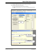

Quick Start Instructions
© 2007 Microchip Technology Inc. DS51669A-page 19
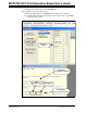
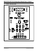
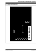
1.3.3 Examples of the MCP4725 Programming
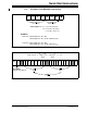
FIGURE 1-3: MCP4725 Device Address Byte.
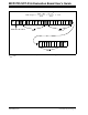
FIGURE 1-4: Fast Mode (Write Command) for V
OUT
= 2.5V when V
REF
= 5V.
1 1 0 0 A2 A1 A0 R/W
Device Code Address Byte *
* Address Byte: A2 = A1 = 0 for Default Samples
A0 = 0 if A0 pin is Grounded
= 1 if A0 pin is tied to V
DD
EXAMPLE:
Write Mode: 0XC0 FOR (A2 = A1 = A0)
0XC2 FOR (A2 = A1 = 0, A0 = TIED TO V
DD
)
Read Mode: 0XC1 FOR (A2 = A1 = A0)
0XC3 FOR (A2 = A1 = 0, A0 = TIED TO V
DD
)
D1D2
0x08
0x00
2
11
=
Address Byte:
when A2 = A1 = A0 = 0
DAC Output
V
REF
D
N
×
4096
--------------------------
5V 2
11
×
4096
--------------------- 2.5V===
ACKStart 00xC0 0 PD1 PD0 D11 D10 D9 D8 D8 D7 D5D6 D4 D3 D0 STOP
ACK
ACK