
User manual

Installation and Operation
© 2010 Microchip Technology Inc. DS51929A-page 19
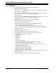
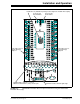
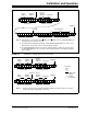
FIGURE 2-4: MCP46XX I
2
C Single Read Command Format.
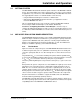
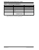
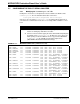
FIGURE 2-5: MCP46XX I
2
C Single Increment / Decrement Command Format.
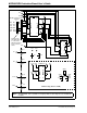
STOP bit
Control Byte
READ Command
1010SA2A1A00 1
AD
AD
AD
AD
A1xXASr
0
1
2
3
Fixed
Address
Variable
Address
Device
Memory
Address
Command
Control Byte Read bits
P
000 00 00D8A
1
Write bit
D3D7 D6 D5 D4 D2 D1 D0 A
2
1010 A2A1A01 A
Read bit
Repeated Start bit
Read Data bits
Note 1: Master Device is responsible for A / A signal. If an A signal occurs, the MCP45XX/46XX will
abort this transfer and release the bus.
2: The Master Device will Not Acknowledge, and the MCP45XX/46XX will release the bus so the
Master Device can generate a Stop or Repeated Start condition.
3: The MCP45XX/46XX retains the last “Device Memory Address” that it has received. This is
the MCP45XX/46XX does not “corrupt” the “Device Memory Address” after Repeated Start or
Stop conditions.
Control Byte
DECR Command
1010SA2A1A00 1
AD
AD
AD
AD
A0XXAP
0
1
23
Fixed
Address
Variable
Address
Device
Memory
Address
Command
Write bit
Note 1: Increment and Decrement Commands (INCR or DECR) only function when accessing the
volatile wiper registers (AD3:AD0 = 0h and 1h).
STOP bit
0 0 = Write Data
0 1 = INCR
1 0 = DECR
1 1 = Read Data
C C
1 0
Command
Bits
Control Byte
INCR Command
1010SA2A1A00 0
AD AD
AD
AD
A1xXAP
0
1
2
3
Fixed
Address
Variable
Address
Device
Memory
Address
Command
Write bit
STOP bit