
User manual

MCP46XXEV Evaluation Board User’s Guide
DS51929A-page 18 © 2010 Microchip Technology Inc.
2.4.2 The MCP4661 Device
To make variations to the commands sent to the MCP4661 device (from the commands
shown in the demo section), one must know the device memory map (see Table 2-3)
and the command formats (see Figure 2-3 through Figure 2-5). For additional device
operational information, refer to the MCP4661 device data sheet (DS22107).
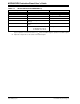
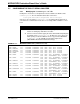
TABLE 2-3: MEMORY MAP AND THE SUPPORTED COMMANDS
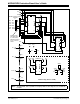
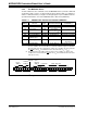
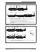
FIGURE 2-3: MCP46XX I
2
C Single Write Command Format.
Address Function
Memory
Type
Allowed Commands
Disallowed
Commands
(2)
00h Volatile Wiper 0 RAM Read, Write,
Increment, Decrement
—
01h Volatile Wiper 1 RAM Read, Write,
Increment, Decrement
—
02h Non-Volatile Wiper 0 EEPROM Read, Write
(1)
Increment, Decrement
03h Non-Volatile Wiper 1 EEPROM Read, Write
(1)
Increment, Decrement
04h Volatile
TCON Register
RAM Read, Write Increment, Decrement
05h Status Register RAM Read Write, Increment,
Decrement
06h - 0Fh Data EEPROM EEPROM Read, Write
(1)
Increment, Decrement
Note 1: When an EEPROM write is active, these are invalid commands and will generate
an error condition. The user should use a read of the STATUS register to determine
when the write cycle has completed. To exit the error condition, the user must take
the CS
pin to the V
IH
level and then back to the active state (V
IL
or V
IHH
).
2: This command on this address will generate an error condition. To exit the error
condition, the user must take the CS
pin to the V
IH
level and then back to the active
state (V
IL
or V
IHH
).
Control Byte
WRITE Command Write Data bits
1010SA2A1A00 0
AD AD
AD
AD
A0xD8AD3D7 D6 D5 D4 D2 D1 D0 A P
0123
Fixed
Address
Variable
Address
Device
Memory
Address
Command
Write “Data” bits
Write bit