
Datasheet


MCP454X/456X/464X/466X
DS22107B-page 48 2008-2013 Microchip Technology Inc.
6.2 I
2
C Operation
The MCP45XX/46XX’s I
2
C module is compatible with
the Philips I
2
C specification. The following lists some of
the modules features:
• 7-bit slave addressing
• Supports three clock rate modes:
- Standard mode, clock rates up to 100 kHz
- Fast mode, clock rates up to 400 kHz
- High-speed mode (HS mode), clock rates up
to 3.4 MHz
• Support Multi-Master Applications
• General call addressing
• Internal weak pull-ups on interface signals
The I
2
C 10-bit addressing mode is not supported.
The Philips I
2
C specification only defines the field
types, field lengths, timings, etc. of a frame. The frame
content defines the behavior of the device. The frame
content for the MCP4XXX is defined in Section 7.0.
6.2.1 I
2
C BIT STATES AND SEQUENCE
Figure 6-8 shows the I
2
C transfer sequence. The serial
clock is generated by the master. The following defini-
tions are used for the bit states:
• Start bit (S)
• Data bit
• Acknowledge (A) bit (driven low) /
No Acknowledge (A
) bit (not driven low)
• Repeated Start bit (Sr)
• Stop bit (P)
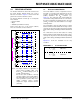
6.2.1.1 Start Bit
The Start bit (see Figure 6-2) indicates the beginning of
a data transfer sequence. The Start bit is defined as the
SDA signal falling when the SCL signal is “High”.
FIGURE 6-2: Start Bit.
6.2.1.2 Data Bit
The SDA signal may change state while the SCL signal
is Low. While the SCL signal is High, the SDA signal
MUST be stable (see Figure 6-5).
FIGURE 6-3: Data Bit.
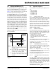
6.2.1.3 Acknowledge (A) Bit
The A bit (see Figure 6-4) is typically a response from
the receiving device to the transmitting device.
Depending on the context of the transfer sequence, the
A bit may indicate different things. Typically the Slave
device will supply an A response after the Start bit and
eight “data” bits have been received. An A bit has the
SDA signal low.
FIGURE 6-4: Acknowledge Waveform.
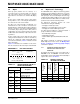
Not A (A) Response
The A bit has the SDA signal high. Table 6-1 shows
some of the conditions where the Slave Device will
issue a Not A (A).
If an error condition occurs (such as an A
instead of A),
then an START bit must be issued to reset the
command state machine.
TABLE 6-1: MCP45XX/MCP46XX A / A
RESPONSES
SDA
SCL
S
1st Bit
2nd Bit
SDA
SCL
Data Bit
1st Bit
2nd Bit
Event
Acknowledge
Bit
Response
Comment
General Call A Only if GCEN bit is
set
Slave Address
valid
A
Slave Address
not valid
A
Device Mem-
ory Address
and specified
command
(AD3:AD0 and
C1:C0) are an
invalid combi-
nation
A
After device has
received address
and command
Communica-
tion during
EEPROM write
cycle
A After device has
received address
and command,
and valid condi-
tions for EEPROM
write
Bus Collision N.A. I
2
C Module
Resets, or a “Don’t
Care” if the colli-
sion occurs on the
Masters “Start bit”.
A
8
D0
9
SDA
SCL