
Datasheet


2008-2013 Microchip Technology Inc. DS22096B-page 97
MCP453X/455X/463X/465X
B.2 Optimizing Circuit Design for Low-
Voltage Characteristics
The low-voltage nonlinear characteristics can be
minimized by application design. The section will show
two application circuits that can be used to control a
programmable reference voltage (V
OUT
).
Minimizing the low-voltage nonlinear characteristics is
done by keeping the voltages on the wiper switch
nodes at a voltage where either the NMOS or PMOS
transistor is turned on.
An example of this is if we are using a digital potentiom-
eter for a voltage reference (V
OUT
). Let’s say that we
want V
OUT
to range from 0.5 * V
DD
to 0.6 * V
DD
.
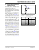
In example implementation #1 (Figure B-15), we
window the digital potentiometer using resistors R1 and
R2. When the wiper code is at full scale, the V
OUT
voltage will be 0.6 * V
DD,
and when the wiper code is
at zero scale, the V
OUT
voltage will be 0.5 * V
DD
.
Remember that the digital potentiometers R
AB
variation
must be included. Table B-1 shows that the V
OUT
volt-
age can be selected to be between 0.455 * V
DD
and
0.727 * V
DD
, which includes the desired range. With
respect to the voltages on the resistor network node, at
1.8V the V
A
voltage would range from 1.29V to 1.31V,
while the V
B
voltage would range from 0.82V to 0.86V.
These voltages cause the wiper resistance to be in the
nonlinear region (see Figure B-12). In Potentiometer
mode, the variation of the wiper resistance is typically
not an issue, as shown by the INL/DNL graph
(Figure 2-7).
In example implementation #2 (Figure B-16), we use
the digital potentiometer in Rheostat mode. The resis-
tor ladder uses resistors R1 and R2 with R
BW
at the
bottom of the ladder. When the wiper code is at full
scale, the V
OUT
voltage will be 0.6 * V
DD
, and when
the wiper code is at full scale, the V
OUT
voltage will be
0.5 * V
DD
. Remember that the digital potentiometers
R
AB
variation must be included. Ta bl e B -2 shows that
the V
OUT
voltage can be selected to be between
0.50 * V
DD
and 0.687 * V
DD
, which includes the desired
range. With respect to the voltages on the resistor net-
work node, at 1.8V the V
W
voltage would range from
0.29V to 0.38V. These voltages cause the wiper
resistance to be in the linear region (see Figure B-12).
FIGURE B-15: Example Implementation #1.
TABLE B-1: EXAMPLE #1 VOLTAGE
CALCULATIONS
Variation
Min Typ Max
R1 12,000 12,000 12,000
R2 20,000 20,000 20,000
R
AB
8,000 10,000 12,000
V
OUT
(@ FS) 0.714 V
DD
0.70 V
DD
0.727 V
DD
V
OUT
(@ ZS) 0.476 V
DD
0.50 V
DD
0.455 V
DD
V
A
0.714 V
DD
0.70 V
DD
0.727 V
DD
V
B
0.476 V
DD
0.50 V
DD
0.455 V
DD
Legend: FS – Full Scale, ZS – Zero Scale
A
B
W
V
W
V
A
V
B
R1
R2
V
OUT