
Datasheet


MCP453X/455X/463X/465X
DS22096B-page 94 2008-2013 Microchip Technology Inc.
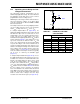
Figure B-3 and Figure B-4 show the wiper resistance
for V
DD
voltages of 5.5, 3.0, 1.8 volts. These graphs
show that as the resistor ladder wiper node voltage
(V
WCn
) approaches the V
DD
/2 voltage, the wiper
resistance increases. These graphs also show the
different resistance characteristics of the NMOS and
PMOS transistors that make up the wiper switch. This
is demonstrated by the wiper code resistance curve,
which does not mirror itself around the mid-scale code
(wiper code = 128).
So why are the R
W
graphs showing the maximum
resistance at about mid-scale (wiper code = 128) and
the R
BW
graphs showing the issue at code 160?
This requires understanding low-voltage transistor
characteristics as well as how the data was measured.
FIGURE B-3: Wiper Resistance (R
W
) vs.
Wiper Code and Temperature
(V
DD
= 5.5V, I
W
= 900 UA; V
DD
= 3.0V,
I
W
= 480 µA).
FIGURE B-4: Wiper Resistance (R
W
) vs.
Wiper Code and Temperature
(V
DD
= 1.8V, I
W
= 260 µA).
The method in which the data was collected is
important to understand. Figure B-5 shows the
technique that was used to measure the R
BW
and R
W
resistance. In this technique, Terminal A is floating and
Terminal B is connected to ground. A fixed current is
then forced into the wiper (I
W
), and the corresponding
wiper voltage (V
W
) is measured. Forcing a known
current through R
BW
(I
W
) and then measuring the
voltage difference between the wiper (V
W
) and
Terminal A (V
A
), the wiper resistance (R
W
) can be
calculated, as shown in Figure B-5. Changes in I
W
cur-
rent will change the wiper voltage (V
W
). This may effect
the device’s wiper resistance (R
W
).
FIGURE B-5: R
BW
and R
W
Measurement.
Figure B-6 shows a block diagram of the resistor
network where the R
AB
resistor is a series of 256 R
S
resistors. These resistors are polysilicon devices. Each
wiper switch is an analog switch made up of an NMOS
and PMOS transistor. A more detailed figure of the
wiper switch is shown in Figure B-7. The wiper
resistance is influenced by the voltage on the wiper
switches’ nodes (V
G
, V
W
and V
WCn
). Temperature also
influences the characteristics of the wiper switch, as
shown in Figure B-4.
The NMOS transistor and PMOS transistor have
different characteristics. These characteristics, as well
as the wiper switch node voltages, determine the R
W
resistance at each wiper code. The variation of each
wiper switch’s characteristics in the resistor network is
greater then the variation of the R
S
resistors.
The voltage on the resistor network node (V
WCn
) is
dependent upon the wiper code selected and the
voltages applied to V
A
, V
B
and V
W
. The wiper switch V
G
voltage to V
W
or V
WCn
voltage determines how strongly
the transistor is turned on. When the transistor is
weakly turned on the wiper resistance, R
W
will be high.
When the transistor is strongly turned on, the wiper
resistance (R
W
) will be in the typical range.
20
40
60
80
100
120
140
160
180
200
220
0 64 128 192 256
Wiper Code
Resistance ()
-40C @ 3.0V +25C @ 3.0V +85C @ 3.0V +125C @ 3.0V
-40C @5.5V +25C @ 5.5V +85C @ 5.5V +125C @ 5.5V
20
520
1020
1520
2020
0 64 128 192 256
Wiper Code
Resistance ()
-40C @ 1.8V
+25C @ 1.8V
+85C @ 1.8V
+125C @ 1.8V
A
B
W
I
W
V
W
floating
R
BW
= V
W
/I
W
V
A
V
B
R
W
= (V
W
-V
A
)/I
W