
Datasheet


2008-2013 Microchip Technology Inc. DS22096B-page 11
MCP453X/455X/463X/465X
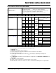
Digital Inputs/Outputs (SDA, SCK, HVC/A0, A1, A2, WP)
Schmitt Trigger High
Input Threshold
V
IH
0.45 V
DD
—— V All
Inputs
except
SDA
and
SCL
2.7V V
DD
5.5V
(Allows 2.7V Digital V
DD
with
5V Analog V
DD
)
0.5 V
DD
—— V 1.8V V
DD
2.7V
0.7 V
DD
—V
MAX
V
SDA
and
SCL
100 kHz
0.7 V
DD
—V
MAX
V400kHz
0.7 V
DD
—V
MAX
V1.7MHz
0.7 V
DD
—V
MAX
V3.4Mhz
Schmitt Trigger Low
Input Threshold
V
IL
— — 0.2V
DD
V All inputs except SDA and SCL
-0.5 — 0.3V
DD
V
SDA
and
SCL
100 kHz
-0.5 — 0.3V
DD
V400kHz
-0.5 — 0.3V
DD
V1.7MHz
-0.5 — 0.3V
DD
V3.4Mhz
Hysteresis of Schmitt
Trigger Inputs (Note 6)
V
HYS
—0.1V
D
D
— V All inputs except SDA and SCL
N.A. — — V
SDA
and
SCL
100 kHz
V
DD
< 2.0V
N.A. — — V V
DD
2.0V
0.1 V
DD
—— V
400 kHz
V
DD
< 2.0V
0.05 V
DD
—— V V
DD
2.0V
0.1 V
DD
—— V 1.7MHz
0.1 V
DD
—— V 3.4Mhz
High Voltage Limit V
MAX
——12.5
(6)
V Pin can tolerate V
MAX
or less.
AC/DC CHARACTERISTICS (CONTINUED)
DC Characteristics
Standard Operating Conditions (unless otherwise specified)
Operating Temperature –40°C T
A
+125°C (extended)
All parameters apply across the specified operating ranges unless noted.
V
DD
= +2.7V to 5.5V, 5 k, 10 k, 50 k, 100 k devices.
Typical specifications represent values for V
DD
= 5.5V, T
A
= +25°C.
Parameters Sym Min Typ Max Units Conditions
Note 1: Resistance is defined as the resistance between terminal A to terminal B.
2: INL and DNL are measured at V
W
with V
A
= V
DD
and V
B
= V
SS
.
3: MCP4XX1 only.
4: MCP4XX2 only, includes V
WZSE
and V
WFSE
.
5: Resistor terminals A, W and B’s polarity with respect to each other is not restricted.
6: This specification by design.
7: Non-linearity is affected by wiper resistance (R
W
), which changes significantly overvoltage and
temperature.
8: The MCP4XX1 is externally connected to match the configurations of the MCP45X2 and MCP46X2, and
then tested.
9: POR/BOR is not rate dependent.
10: Supply current is independent of current through the resistor network.
11: When HVC/A0 = V
IHH
, the I
DD
current is less due to current into the HVC/A0 pin. See I
PU
specification.