
User manual

Installation and Operation
© 2010 Microchip Technology Inc. DS51892A-page 27
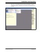
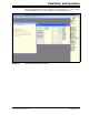
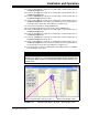
Double clicking on the ReadWiper0 User SPI Script will load the Script Details.
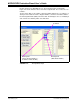
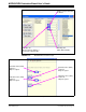
Figure 2-11 shows what the values mean in the Script Details. These values are hex
numbers.
The first value (02h), is the number of bytes that will be written. The second byte is a
data byte and contains the Device Register Address, the Device Command, and the
two Most Significant bits (MSb) of the read data. The third byte is the second data byte
and contains the remaining 8 bits of the read data.
During read commands, the value of the two LSbs of Data Byte #1 and all of the bits of
Data Byte #2 are not important. The bytes are required for the SPI clock generation.
FIGURE 2-11: Example Read Script.
Number of Bytes that will
be written
Data Byte #2
(Write Data “D7:D0”)
Data Byte #1
(Device Register Address +
Command + Data bit “D8”)