
User manual

Installation and Operation
2010 Microchip Technology Inc. DS51898A-page 17
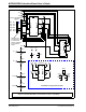
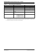
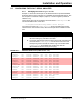
TABLE 2-2: OPTIONAL PASSIVE COMPONENTS – NOT INSTALLED
(2)
Component Comment
C1, C2 Power supply bypass capacitors
(3)
C3, C4 PIC
®
MCU Crystal capacitors
R1U, R2U, R3U, R4U, R5U, R6U, R7U, R8U,
R9U, R12U, R13U, R16U, R18U, R19U, R20U
Pull-up resistor
R1D, R2D, R3D, R4D, R5D, R6D, R8D, R9D,
R10D, R11D, R12D, R14D, R15D, R16D, R17D,
R18D, R19D, R20D
Pull-down resistor
(1)
U1, U2 Alternate package footprints
VDD, GND Power and Ground plane connection
points
Y1 Can connect to either PIC
®
MCUs main
oscillator or to the Timer oscillator circuit.
P1, P2, P3, P4, P5, P6, P8, P10, P11, P13, P14,
P15, P16, P17, P18, P19, P20
Test Point connectors
Note 1: Whichever pin is the device’s V
DD
pin, that corresponding RXD footprint can be
used for the device’s bypass capacitor. So if Pin 8 is the device’s V
DD
pin, then
install the bypass capacitor in the R8D footprint.
2: All passive components use the surface mount 805 footprint.
3: If the board is powered via the V
DD
and GND connection points, the use of bypass
capacitors on C1 and C2 may improve performance. The benefit is reduced if the
board is powered via the PICkit™ serial interface.