
User manual

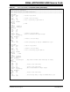

00066_MCP402XEV.ASM Source Code
© 2005 Microchip Technology Inc. DS51546B-page 40
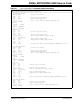
DLOOP_HVIWL
clrwdt ;or NOP
nop
decfsz DLYCNT1,f
goto DLOOP_HVIWL
bcf UD
goto $+1 ; creates a 3us total delay
bsf UD
goto $+1 ; creates a 3us total delay
bcf UD
goto $+1 ; creates a 3us total delay
bcf HV_CS ; shut off 1Mhz Charge Pump
bcf CS ; helps pull the signal down from HV
goto $+1
bsf CS
retlw 0x04 ; Follow w/long delay to discharge pump & EEPROM Write Cycle
HV_Decrement_WL_Enable
bcf UD
bsf CS
goto $+1 ; creates a 3us total delay
bsf HV_CS ; starts 1Mhz Charge Pump
movlw .100 ; 5*100 = 500us delay for Charge Pump ramp time
movwf DLYCNT1
DLOOP_HVDWL
clrwdt ;or NOP
nop
decfsz DLYCNT1,f
goto DLOOP_HVDWL
bsf UD
goto $+1 ; creates a 3us total delay
bcf HV_CS ; shut off 1Mhz Charge Pump
bcf CS ; helps pull the signal down from HV
goto $+1
bsf CS
retlw 0x05 ; Follow w/long delay to discharge pump & EEPROM Write Cycle
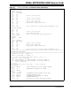
;***********************************************************************************************
; VARIABLE DELAY SUBROUTINES
;***********************************************************************************************
; DLYCNT1 = F9h = 249d DLYCNT2 = W
; DELAY = T((4 DLYCNT1 + 4) DLYCNT2 + 4)
;
; ex. To create a 300ms delay when using a 4Mhz osc, 300-250 = 50
; movlw .50 ;load .50 into WREG
; call VAR1000TcyDELAY ;call VAR1000TcyDELAY = 50ms delay w/4MHz Osc
; call VAR1000TcyDELAY ;call VAR1000TcyDELAY = 250ms delay w/4MHz Osc
; ;total = 300ms delay
;************
; The value in W at the time of the CALL = x. Delay = 1000Tcy*x
VAR1000TcyDELAY
movwf DLYCNT2 ; LOADS CONTROLLING DLY # INTO PRIMARY COUNTER
DLOOP2
movlw .249 ; MAXIMIZES THE SECONDARY DLY COUNTER
movwf DLYCNT1
DLOOP1
clrwdt ;or NOP
decfsz DLYCNT1,f ; DECREMENT AND TEST SECONDARY LOOP FOR ZERO
goto DLOOP1 ; CONTINUE SECONDARY LOOP
decfsz DLYCNT2,f ; DECREMENT AND TEST PRIMARY DLY COUNTER
goto DLOOP2 ; CONTINUE PRIMARY LOOP
retlw .250 ; preload W for the next CALL VAR1000TcyDELAY
TABLE E-1: 00066_MCP402XEV.ASM SOURCE CODE (CONTINUED)