
Datasheet


Table Of Contents
- MCP3905A/05L/06A
- Features
- Description
- Package Type
- Functional Block Diagram
- Notes:
- 1.0 Electrical Characteristics
- 2.0 Typical Performance Curves
- FIGURE 2-1: Measurement Error, Gain = 8 PF = 1.
- FIGURE 2-2: Measurement Error, Gain = 16, PF = 1.
- FIGURE 2-3: Measurement Error, Gain = 32, PF = 1.
- FIGURE 2-4: Measurement Error, Gain = 8, PF = 0.5.
- FIGURE 2-5: Measurement Error, Gain = 16, PF = 0.5.
- FIGURE 2-6: Measurement Error, Gain =32, PF = 0.5.
- FIGURE 2-7: Measurement Error, Gain = 1, PF = 1.
- FIGURE 2-8: Measurement Error, Gain = 2, PF = 1.
- FIGURE 2-9: Measurement Error, Gain = 1, PF = + 0.5.
- FIGURE 2-10: Measurement Error, Gain = 2, PF = + 0.5.
- FIGURE 2-11: Measurement Error, Temperature = +125°C, Gain = 1.
- FIGURE 2-12: Measurement Error, Temperature = +125°C, Gain = 2.
- FIGURE 2-13: Measurement Error, Temperature = +125°C, Gain = 8.
- FIGURE 2-14: Measurement Error, Temperature = +125°C, Gain = 16.
- FIGURE 2-15: Measurement Error vs. Input Frequency.
- FIGURE 2-16: Channel 0 Offset Error (DC Mode, HPF off), G = 1.
- FIGURE 2-17: Channel 0 Offset Error (DC Mode, HPF off), G = 8.
- FIGURE 2-18: Channel 0 Offset Error (DC Mode, HPF Off), G = 16.
- FIGURE 2-19: Measurement Error vs. VDD (G = 16).
- FIGURE 2-20: Measurement Error vs. VDD, G = 16, External VREF.
- FIGURE 2-21: Measurement Error w/ External VREF, (G = 1).
- FIGURE 2-22: Measurement Error w/ External VREF (G = 8).
- FIGURE 2-23: Measurement Error w/ External VREF (G = 16).
- 3.0 Pin Descriptions
- TABLE 3-1: Pin Function Table
- 3.1 Digital VDD (DVDD)
- 3.2 High-Pass Filter Input Logic Pin (HPF)
- 3.3 Analog VDD (AVDD)
- 3.4 Current Channel (CH0-, CH0+)
- 3.5 Voltage Channel (CH1-,CH1+)
- 3.6 Master Clear (MCLR)
- 3.7 Reference (REFIN/OUT)
- 3.8 Analog Ground (AGND)
- 3.9 Frequency Control Logic Pins (F2, F1, F0)
- 3.10 Gain Control Logic Pins (G1, G0)
- 3.11 Oscillator (OSC1, OSC2)
- 3.12 Negative Power Output Logic Pin (NEG)
- 3.13 Ground Connection (DGND)
- 3.14 High-Frequency Output (HFOUT)
- 3.15 Frequency Output (FOUT0, FOUT1)
- 4.0 Device Overview
- 5.0 Applications Information
- 6.0 Packaging Information
- Trademarks
- Worldwide Sales and Service
© 2006-2011 Microchip Technology Inc. DS22011B-page 7
MCP3905A/05L/06A
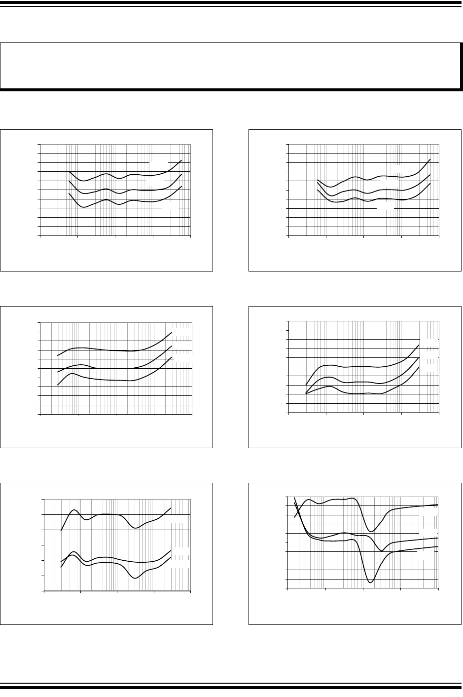
2.0 TYPICAL PERFORMANCE CURVES
Note: Unless otherwise specified, DV
DD
, AV
DD
= 5V; A
GND
, D
GND
= 0V; V
REF
= Internal, HPF = 1 (AC mode),
MCLK = 3.58 MHz.
FIGURE 2-1: Measurement Error,
Gain = 8 PF = 1.
FIGURE 2-2: Measurement Error,
Gain = 16, PF = 1.
FIGURE 2-3: Measurement Error,
Gain = 32, PF = 1.
FIGURE 2-4: Measurement Error,
Gain = 8, PF = 0.5.
FIGURE 2-5: Measurement Error,
Gain = 16, PF = 0.5.
FIGURE 2-6: Measurement Error,
Gain =32, PF = 0.5.
Note: The graphs and tables provided following this note are a statistical summary based on a limited number of
samples and are provided for informational purposes only. The performance characteristics listed herein
are not tested or guaranteed. In some graphs or tables, the data presented may be outside the specified
operating range (e.g., outside specified power supply range) and therefore outside the warranted range.
-0.5
-0.4
-0.3
-0.2
-0.1
0
0.1
0.2
0.3
0.4
0.5
0.0000 0.0001 0.0010 0.0100 0.1000
CH1 Vp-p Amplitude (V)
Measurement Error
+85°C
+25°C
-40°C
`
-0.5
-0.4
-0.3
-0.2
-0.1
0
0.1
0.2
0.3
0.4
0.5
0.0000 0.0001 0.0010 0.0100 0.1000
CH1 Vp-p Amplitude (V)
Measurement Error
+85°C
+25°C
- 40°C
-0.5
-0.25
0
0.25
0.5
0.75
1
0.0000 0.0001 0.0010 0.0100 0.1000
CH1 Vp-p Amplitude (V)
Measurement Error
+85°C
+25°C
- 40°C
-0.5
-0.4
-0.3
-0.2
-0.1
0
0.1
0.2
0.3
0.4
0.5
0.0000 0.0001 0.0010 0.0100 0.1000
CH1 Vp-p Amplitude (V)
Measurement Error
+85°C
+25°C
-40°C
-0.5
-0.4
-0.3
-0.2
-0.1
0
0.1
0.2
0.3
0.4
0.5
0.0000 0.0001 0.0010 0.0100 0.1000
CH1 Vp-p Amplitude (V)
Measurement Error
+85°C
+25°C
-40°C
-1
-0.8
-0.6
-0.4
-0.2
0
0.2
0.4
0.6
0.8
1
0.0000 0.0001 0.0010 0.0100 0.1000
CH1 Vp-p Amplitude (V)
Measurement Error
+85°C
+25°C
-40°C