
Datasheet


Table Of Contents
- MCP3905A/05L/06A
- Features
- Description
- Package Type
- Functional Block Diagram
- Notes:
- 1.0 Electrical Characteristics
- 2.0 Typical Performance Curves
- FIGURE 2-1: Measurement Error, Gain = 8 PF = 1.
- FIGURE 2-2: Measurement Error, Gain = 16, PF = 1.
- FIGURE 2-3: Measurement Error, Gain = 32, PF = 1.
- FIGURE 2-4: Measurement Error, Gain = 8, PF = 0.5.
- FIGURE 2-5: Measurement Error, Gain = 16, PF = 0.5.
- FIGURE 2-6: Measurement Error, Gain =32, PF = 0.5.
- FIGURE 2-7: Measurement Error, Gain = 1, PF = 1.
- FIGURE 2-8: Measurement Error, Gain = 2, PF = 1.
- FIGURE 2-9: Measurement Error, Gain = 1, PF = + 0.5.
- FIGURE 2-10: Measurement Error, Gain = 2, PF = + 0.5.
- FIGURE 2-11: Measurement Error, Temperature = +125°C, Gain = 1.
- FIGURE 2-12: Measurement Error, Temperature = +125°C, Gain = 2.
- FIGURE 2-13: Measurement Error, Temperature = +125°C, Gain = 8.
- FIGURE 2-14: Measurement Error, Temperature = +125°C, Gain = 16.
- FIGURE 2-15: Measurement Error vs. Input Frequency.
- FIGURE 2-16: Channel 0 Offset Error (DC Mode, HPF off), G = 1.
- FIGURE 2-17: Channel 0 Offset Error (DC Mode, HPF off), G = 8.
- FIGURE 2-18: Channel 0 Offset Error (DC Mode, HPF Off), G = 16.
- FIGURE 2-19: Measurement Error vs. VDD (G = 16).
- FIGURE 2-20: Measurement Error vs. VDD, G = 16, External VREF.
- FIGURE 2-21: Measurement Error w/ External VREF, (G = 1).
- FIGURE 2-22: Measurement Error w/ External VREF (G = 8).
- FIGURE 2-23: Measurement Error w/ External VREF (G = 16).
- 3.0 Pin Descriptions
- TABLE 3-1: Pin Function Table
- 3.1 Digital VDD (DVDD)
- 3.2 High-Pass Filter Input Logic Pin (HPF)
- 3.3 Analog VDD (AVDD)
- 3.4 Current Channel (CH0-, CH0+)
- 3.5 Voltage Channel (CH1-,CH1+)
- 3.6 Master Clear (MCLR)
- 3.7 Reference (REFIN/OUT)
- 3.8 Analog Ground (AGND)
- 3.9 Frequency Control Logic Pins (F2, F1, F0)
- 3.10 Gain Control Logic Pins (G1, G0)
- 3.11 Oscillator (OSC1, OSC2)
- 3.12 Negative Power Output Logic Pin (NEG)
- 3.13 Ground Connection (DGND)
- 3.14 High-Frequency Output (HFOUT)
- 3.15 Frequency Output (FOUT0, FOUT1)
- 4.0 Device Overview
- 5.0 Applications Information
- 6.0 Packaging Information
- Trademarks
- Worldwide Sales and Service
© 2006-2011 Microchip Technology Inc. DS22011B-page 5
MCP3905A/05L/06A
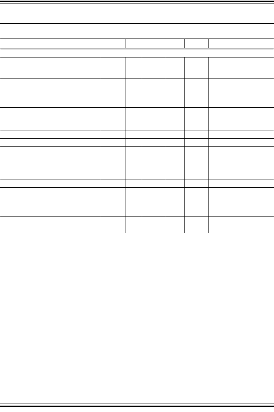
TIMING CHARACTERISTICS
Electrical Specifications: Unless otherwise indicated, all parameters apply at AV
DD
= DV
DD
= 4.5V – 5.5V,
A
GND
, D
GND
= 0V, MCLK = 3.58 MHz; T
A
= -40°C to +85°C.
Parameter Sym Min Typ Max Units Comment
Frequency Output
F
OUT0
and F
OUT1
Pulse Width
(Logic Low) for MCP3905A, MCP3906A
devices
t
FW
—
275
—
ms 984376 MCLK periods
(Note 1)
HF
OUT
Pulse Width for MCP3905A,
MCP3906A devices
t
HW
—
90
—
ms 322160 MCLK periods
(Note 2)
F
OUT0
and F
OUT1
Pulse Width
(Logic Low) for MCP3905L device
t
FW
—
130
—
ms 465344 MCLK periods
(Note 1)
HF
OUT
Pulse Width for MCP3905L
device
t
HW
—
65
—
ms 232672 MCLK periods
(Note 2)
F
OUT0
and F
OUT1
Pulse Period t
FP
Refer to Equation 4-1 s
HF
OUT
Pulse Period t
HP
Refer to Equation 4-2 s
F
OUT0
to F
OUT1
Falling-Edge Time t
FS2
—
0.5 t
FP
—
F
OUT0
to F
OUT1
Min Separation t
FS
—
4/MCLK
—
F
OUT0
and F
OUT1
Output High Voltage V
OH
4.5
——
VI
OH
= 10 mA, DV
DD
= 5.0V
F
OUT0
and F
OUT1
Output Low Voltage V
OL
——
0.5 V I
OL
= 10 mA, DV
DD
= 5.0V
HF
OUT
Output High Voltage V
OH
4.0
——
VI
OH
= 5 mA, DV
DD
= 5.0V
HF
OUT
Output Low Voltage V
OL
——
0.5 V I
OL
= 5 mA, DV
DD
= 5.0V
High-Level Input Voltage
(All Digital Input Pins)
V
IH
2.4
——
VDV
DD
= 5.0V
Low Level Input Voltage
(All Digital Input Pins)
V
IL
——
0.85 V DV
DD
= 5.0V
Input Leakage Current
——
±3 µA V
IN
= 0, V
IN
= DV
DD
Pin Capacitance
——
10 pF Note 3
Note 1: If output pulse period (t
FP
) falls below 984376*2 MCLK periods for MCP3905A/6A and 465344*2 MCLK
periods for MCP3905L, then t
FW
= 1/2 t
FP
.
2: If output pulse period (t
HP
) falls below 322160*2 MCLK periods for MCP3905A/6A and 232672*2 MCLK
periods for MCP3905L, then t
HW
= 1/2 t
HP
. When F2, F1,F0 = 011, t
HW
is fixed to 18 µs (64 MCLK
periods).
3: Specified by characterization, not production tested.