
Datasheet


Table Of Contents
- MCP3905A/05L/06A
- Features
- Description
- Package Type
- Functional Block Diagram
- Notes:
- 1.0 Electrical Characteristics
- 2.0 Typical Performance Curves
- FIGURE 2-1: Measurement Error, Gain = 8 PF = 1.
- FIGURE 2-2: Measurement Error, Gain = 16, PF = 1.
- FIGURE 2-3: Measurement Error, Gain = 32, PF = 1.
- FIGURE 2-4: Measurement Error, Gain = 8, PF = 0.5.
- FIGURE 2-5: Measurement Error, Gain = 16, PF = 0.5.
- FIGURE 2-6: Measurement Error, Gain =32, PF = 0.5.
- FIGURE 2-7: Measurement Error, Gain = 1, PF = 1.
- FIGURE 2-8: Measurement Error, Gain = 2, PF = 1.
- FIGURE 2-9: Measurement Error, Gain = 1, PF = + 0.5.
- FIGURE 2-10: Measurement Error, Gain = 2, PF = + 0.5.
- FIGURE 2-11: Measurement Error, Temperature = +125°C, Gain = 1.
- FIGURE 2-12: Measurement Error, Temperature = +125°C, Gain = 2.
- FIGURE 2-13: Measurement Error, Temperature = +125°C, Gain = 8.
- FIGURE 2-14: Measurement Error, Temperature = +125°C, Gain = 16.
- FIGURE 2-15: Measurement Error vs. Input Frequency.
- FIGURE 2-16: Channel 0 Offset Error (DC Mode, HPF off), G = 1.
- FIGURE 2-17: Channel 0 Offset Error (DC Mode, HPF off), G = 8.
- FIGURE 2-18: Channel 0 Offset Error (DC Mode, HPF Off), G = 16.
- FIGURE 2-19: Measurement Error vs. VDD (G = 16).
- FIGURE 2-20: Measurement Error vs. VDD, G = 16, External VREF.
- FIGURE 2-21: Measurement Error w/ External VREF, (G = 1).
- FIGURE 2-22: Measurement Error w/ External VREF (G = 8).
- FIGURE 2-23: Measurement Error w/ External VREF (G = 16).
- 3.0 Pin Descriptions
- TABLE 3-1: Pin Function Table
- 3.1 Digital VDD (DVDD)
- 3.2 High-Pass Filter Input Logic Pin (HPF)
- 3.3 Analog VDD (AVDD)
- 3.4 Current Channel (CH0-, CH0+)
- 3.5 Voltage Channel (CH1-,CH1+)
- 3.6 Master Clear (MCLR)
- 3.7 Reference (REFIN/OUT)
- 3.8 Analog Ground (AGND)
- 3.9 Frequency Control Logic Pins (F2, F1, F0)
- 3.10 Gain Control Logic Pins (G1, G0)
- 3.11 Oscillator (OSC1, OSC2)
- 3.12 Negative Power Output Logic Pin (NEG)
- 3.13 Ground Connection (DGND)
- 3.14 High-Frequency Output (HFOUT)
- 3.15 Frequency Output (FOUT0, FOUT1)
- 4.0 Device Overview
- 5.0 Applications Information
- 6.0 Packaging Information
- Trademarks
- Worldwide Sales and Service
MCP3905A/05L/06A
DS22011B-page 18 © 2006-2011 Microchip Technology Inc.
The multiplier output gives the product of the two high-
pass filtered channels, corresponding to instantaneous
real power. Multiplying two sine wave signals by the
same ω frequency gives a DC component and a 2ω
component. The instantaneous power signal contains
the real power of its DC component, while also contain-
ing 2ω components coming from the line frequency
multiplication. These 2ω components come for the line
frequency (and its harmonics) and must be removed in
order to extract the real-power information. This is
accomplished using the low-pass filter and DTF
converter.
4.6 Low-Pass Filter and DTF
Converter
The MCP3905A/05L/06A low-pass filter is a first-order
IIR filter that extracts the active real-power information
(DC component) from the instantaneous power signal.
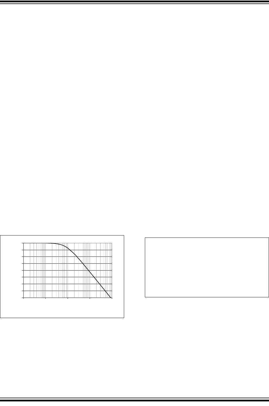
The magnitude response of this filter is detailed in
Figure 4-5. Due to the fact that the instantaneous power
signal has harmonic content (coming from the 2ω
components of the inputs), and since the filter is not
ideal, there will be some ripple at the output of the low-
pass filter at the harmonics of the line frequency.
The cut-off frequency of the filter (8.9 Hz) has been
chosen to have sufficient rejection for commonly-used
line frequencies (50 Hz and 60 Hz). With a standard
input clock (MCLK = 3.58 MHz) and a 50 Hz line
frequency, the rejection of the 2ω component (100 Hz)
will be more than 20 dB. This equates to a 2ω
component containing 10 times less power than the
main DC component (i.e., the average active real
power).
FIGURE 4-5: LPF Magnitude Response
(MCLK = 3.58 MHz).
The output of the low-pass filter is accumulated in the
digital-to-frequency converter. This accumulation is
compared to a different digital threshold for F
OUT0/1
and HF
OUT
, representing a quantity of real energy mea-
sured by the part. Every time the digital threshold on
F
OUT0/1
or HF
OUT
is crossed, the part will output a
pulse (See Section 4.7 “F
OUT0/1
and HF
OUT
Output
Frequencies”).
The equivalent quantity of real energy required to
output a pulse is much larger for the F
OUT0/1
outputs
than the HF
OUT
. This is such that the integration period
for the F
OUT0/1
outputs is much larger. This larger
integration period acts as another low-pass filter so that
the output ripple due to the 2ω components is minimal.
However, these components are not totally removed,
since realized low-pass filters are never ideal. This will
create a small jitter in the output frequency. Averaging
the output pulses with a counter or a MCU in the
application will then remove the small sinusoidal
content of the output frequency and filter out the
remaining 2ω ripple.
HF
OUT
is intended to be used for calibration purposes
due to its instantaneous power content. The shorter
integration period of HF
OUT
demands that the 2ω
component be given more attention. Since a sinusoidal
signal average is zero, averaging the HF
OUT
signal in
steady-state conditions will give the proper real energy
value.
4.7 F
OUT0/1
and HF
OUT
Output
Frequencies
The thresholds for the accumulated energy are
different for F
OUT0/1
and HF
OUT
(i.e., they have
different transfer functions). The F
OUT0/1
allowed
output frequencies are quite low in order to allow
superior integration time (see Section 4.6 “Low-Pass
Filter and DTF Converter”). The F
OUT0/1
output
frequency can be calculated with the following
equation:
EQUATION 4-1: F
OUT
FREQUENCY
OUTPUT EQUATION
For a given DC input V, the DC and RMS values are
equivalent. For a given AC input signal with peak-to-
peak amplitude of V, the equivalent RMS value is
V/sqrt(2), assuming purely sinusoidal signals. Note
that since the real power is the product of two RMS
inputs, the output frequencies of AC signals are half of
the DC inputs ones, again assuming purely sinusoidal
AC signals. The constant F
C
depends on the F
OUT0
and F
OUT1
digital settings. Table 4-3 shows F
OUT0/1
output frequencies for the different logic settings.
-40
-35
-30
-25
-20
-15
-10
-5
0
0.1 1 10 100 1000
Frequency (Hz)
Normal Mode Rejection (dB)
F
OUT
Hz()
8.06 V
0
× V
1
× GF
C
××
V
REF
()
2
-----------------------------------------------------------=
Where:
V
0
is the RMS differential voltage on Channel 0
V
1
is the RMS differential voltage on Channel 1
G is the PGA gain on Channel 0 (current channel)
F
C
is the frequency constant selected
V
REF
is the voltage reference