
Datasheet


Table Of Contents
- MCP3905A/05L/06A
- Features
- Description
- Package Type
- Functional Block Diagram
- Notes:
- 1.0 Electrical Characteristics
- 2.0 Typical Performance Curves
- FIGURE 2-1: Measurement Error, Gain = 8 PF = 1.
- FIGURE 2-2: Measurement Error, Gain = 16, PF = 1.
- FIGURE 2-3: Measurement Error, Gain = 32, PF = 1.
- FIGURE 2-4: Measurement Error, Gain = 8, PF = 0.5.
- FIGURE 2-5: Measurement Error, Gain = 16, PF = 0.5.
- FIGURE 2-6: Measurement Error, Gain =32, PF = 0.5.
- FIGURE 2-7: Measurement Error, Gain = 1, PF = 1.
- FIGURE 2-8: Measurement Error, Gain = 2, PF = 1.
- FIGURE 2-9: Measurement Error, Gain = 1, PF = + 0.5.
- FIGURE 2-10: Measurement Error, Gain = 2, PF = + 0.5.
- FIGURE 2-11: Measurement Error, Temperature = +125°C, Gain = 1.
- FIGURE 2-12: Measurement Error, Temperature = +125°C, Gain = 2.
- FIGURE 2-13: Measurement Error, Temperature = +125°C, Gain = 8.
- FIGURE 2-14: Measurement Error, Temperature = +125°C, Gain = 16.
- FIGURE 2-15: Measurement Error vs. Input Frequency.
- FIGURE 2-16: Channel 0 Offset Error (DC Mode, HPF off), G = 1.
- FIGURE 2-17: Channel 0 Offset Error (DC Mode, HPF off), G = 8.
- FIGURE 2-18: Channel 0 Offset Error (DC Mode, HPF Off), G = 16.
- FIGURE 2-19: Measurement Error vs. VDD (G = 16).
- FIGURE 2-20: Measurement Error vs. VDD, G = 16, External VREF.
- FIGURE 2-21: Measurement Error w/ External VREF, (G = 1).
- FIGURE 2-22: Measurement Error w/ External VREF (G = 8).
- FIGURE 2-23: Measurement Error w/ External VREF (G = 16).
- 3.0 Pin Descriptions
- TABLE 3-1: Pin Function Table
- 3.1 Digital VDD (DVDD)
- 3.2 High-Pass Filter Input Logic Pin (HPF)
- 3.3 Analog VDD (AVDD)
- 3.4 Current Channel (CH0-, CH0+)
- 3.5 Voltage Channel (CH1-,CH1+)
- 3.6 Master Clear (MCLR)
- 3.7 Reference (REFIN/OUT)
- 3.8 Analog Ground (AGND)
- 3.9 Frequency Control Logic Pins (F2, F1, F0)
- 3.10 Gain Control Logic Pins (G1, G0)
- 3.11 Oscillator (OSC1, OSC2)
- 3.12 Negative Power Output Logic Pin (NEG)
- 3.13 Ground Connection (DGND)
- 3.14 High-Frequency Output (HFOUT)
- 3.15 Frequency Output (FOUT0, FOUT1)
- 4.0 Device Overview
- 5.0 Applications Information
- 6.0 Packaging Information
- Trademarks
- Worldwide Sales and Service
MCP3905A/05L/06A
DS22011B-page 16 © 2006-2011 Microchip Technology Inc.
4.1 Analog Inputs
The MCP3905A/05L/06A analog inputs can be
connected directly to the current and voltage
transducers (such as shunts or current transformers).
Each input pin is protected by specialized ESD
structures that are certified to pass 5 kV HBM and
500V MM contact charge. These structures also allow
up to ±6V continuous voltage to be present at their
inputs without the risk of permanent damage.
Both channels have fully differential voltage inputs for
better noise performance. The absolute voltage at each
pin relative to A
GND
should be maintained in the ±1V
range during operation in order to ensure the
measurement error performance. The common-mode
signals should be adapted to respect both the previous
conditions and the differential input voltage range. For
best performance, the common-mode signals should
be referenced to A
GND
.
The current channel comprises a PGA on the front-end
to allow for smaller signals to be measured without
additional signal conditioning. The maximum differen-
tial voltage specified on Channel 0 is equal to
±470 mV/Gain (see Table 4-1). The maximum peak
voltage specified on Channel 1 is equal to ±660 mV.
.
4.2 16-Bit Delta-Sigma A/D Converters
The ADCs used in the MCP3905A/05L/06A for both
current and voltage channel measurements are delta-
sigma ADCs. They comprise a second-order, delta-
sigma modulator using a multi-bit DAC and a third-
order SINC filter. The delta-sigma architecture is very
appropriate for the applications targeted by the
MCP3905A/05L/06A because it is a waveform-oriented
converter architecture that can offer both high linearity
and low distortion performance throughout a wide input
dynamic range. It also creates minimal requirements
for the anti-aliasing filter design. The multi-bit
architecture used in the ADC minimizes quantization
noise at the output of the converters without disturbing
the linearity.
Both ADCs have a 16-bit resolution, allowing wide input
dynamic range sensing. The oversampling ratio of both
converters is 64. Both converters are continuously
converting during normal operation. When the MCLR
pin is low, both converters will be in Reset and output
code 0x0000h. If the voltage at the inputs of the ADC is
larger than the specified range, the linearity is no longer
specified. However, the converters will continue to
produce output codes until their saturation point is
reached. The DC saturation point is around 700 mV for
Channel 0 and 1V for Channel 1, using internal voltage
reference.
The clocking signals for the ADCs are equally
distributed between the two channels in order to
minimize phase delays to less than 1 MCLK period
(see Section 3.2 “High-Pass Filter Input Logic Pin
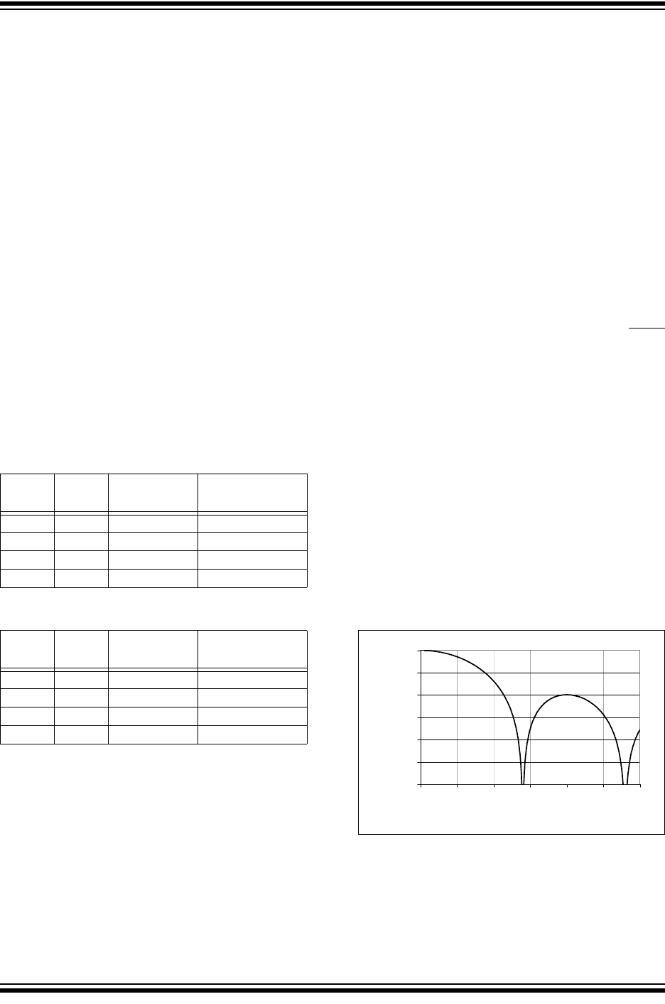
(HPF)”). The SINC filter’s main notch is positioned at
MCLK/256 (14 kHz with MCLK = 3.58 MHz), allowing
the user to be able to measure wide harmonic content
on either channel. The magnitude response of the
SINC filter is shown in Figure 4-2.
FIGURE 4-2: SINC Filter Magnitude
Response (MCLK = 3.58 MHz).
TABLE 4-1: MCP3905A/MCP3905L GAIN
SELECTIONS
G1 G0 CH0 Gain
Maximum
CH0 Voltage
00 1±470mV
01 2±235mV
10 8±60mV
11 16 ±30 mV
TABLE 4-2: MCP3906A GAIN
SELECTIONS
G1 G0 CH0 Gain
Maximum
CH0 Voltage
00 1±470mV
01 32 ±15 mV
10 8±60mV
11 16 ±30 mV
-120
-100
-80
-60
-40
-20
0
0 5 10 15 20 25 30
Frequency (kHz)
Normal Mode Rejection (dB)