
Datasheet


Table Of Contents
- MCP3905A/05L/06A
- Features
- Description
- Package Type
- Functional Block Diagram
- Notes:
- 1.0 Electrical Characteristics
- 2.0 Typical Performance Curves
- FIGURE 2-1: Measurement Error, Gain = 8 PF = 1.
- FIGURE 2-2: Measurement Error, Gain = 16, PF = 1.
- FIGURE 2-3: Measurement Error, Gain = 32, PF = 1.
- FIGURE 2-4: Measurement Error, Gain = 8, PF = 0.5.
- FIGURE 2-5: Measurement Error, Gain = 16, PF = 0.5.
- FIGURE 2-6: Measurement Error, Gain =32, PF = 0.5.
- FIGURE 2-7: Measurement Error, Gain = 1, PF = 1.
- FIGURE 2-8: Measurement Error, Gain = 2, PF = 1.
- FIGURE 2-9: Measurement Error, Gain = 1, PF = + 0.5.
- FIGURE 2-10: Measurement Error, Gain = 2, PF = + 0.5.
- FIGURE 2-11: Measurement Error, Temperature = +125°C, Gain = 1.
- FIGURE 2-12: Measurement Error, Temperature = +125°C, Gain = 2.
- FIGURE 2-13: Measurement Error, Temperature = +125°C, Gain = 8.
- FIGURE 2-14: Measurement Error, Temperature = +125°C, Gain = 16.
- FIGURE 2-15: Measurement Error vs. Input Frequency.
- FIGURE 2-16: Channel 0 Offset Error (DC Mode, HPF off), G = 1.
- FIGURE 2-17: Channel 0 Offset Error (DC Mode, HPF off), G = 8.
- FIGURE 2-18: Channel 0 Offset Error (DC Mode, HPF Off), G = 16.
- FIGURE 2-19: Measurement Error vs. VDD (G = 16).
- FIGURE 2-20: Measurement Error vs. VDD, G = 16, External VREF.
- FIGURE 2-21: Measurement Error w/ External VREF, (G = 1).
- FIGURE 2-22: Measurement Error w/ External VREF (G = 8).
- FIGURE 2-23: Measurement Error w/ External VREF (G = 16).
- 3.0 Pin Descriptions
- TABLE 3-1: Pin Function Table
- 3.1 Digital VDD (DVDD)
- 3.2 High-Pass Filter Input Logic Pin (HPF)
- 3.3 Analog VDD (AVDD)
- 3.4 Current Channel (CH0-, CH0+)
- 3.5 Voltage Channel (CH1-,CH1+)
- 3.6 Master Clear (MCLR)
- 3.7 Reference (REFIN/OUT)
- 3.8 Analog Ground (AGND)
- 3.9 Frequency Control Logic Pins (F2, F1, F0)
- 3.10 Gain Control Logic Pins (G1, G0)
- 3.11 Oscillator (OSC1, OSC2)
- 3.12 Negative Power Output Logic Pin (NEG)
- 3.13 Ground Connection (DGND)
- 3.14 High-Frequency Output (HFOUT)
- 3.15 Frequency Output (FOUT0, FOUT1)
- 4.0 Device Overview
- 5.0 Applications Information
- 6.0 Packaging Information
- Trademarks
- Worldwide Sales and Service
© 2006-2011 Microchip Technology Inc. DS22011B-page 19
MCP3905A/05L/06A
The high-frequency output HF
OUT
has lower
integration times and, thus, higher frequencies. The
output frequency value can be calculated with the
following equation:
EQUATION 4-2: HF
OUT
FREQUENCY
OUTPUT EQUATION
The constant HF
C
depends on the F
OUT0
and F
OUT1
digital settings with the Table 4-4.
The detailed timings of the output pulses are described
in the Timing Characteristics table (see Section 1.0
“Electrical Characteristics” and Figure 1-1).
4.7.1 MINIMAL OUTPUT FREQUENCY
FOR
NO-LOAD THRESHOLD
The MCP3905A/05L/06A devices also include, on
each output frequency, a no-load threshold circuit that
will eliminate any creep effects in the meter. The
outputs will not show any pulse if the output frequency
falls below the no-load threshold. The minimum output
frequency on F
OUT0/1
and HF
OUT
is equal to 0.0015%
of the maximum output frequency (respectively F
C
and
HF
C
) for each of the F2, F1 and F0 selections (see
Table 4-3 and Table 4-4); except when F2, F1,
F0 = 011. In this last configuration, the no-load
threshold feature is disabled. The selection of F
C
will
determine the start-up current load. In order to respect
the IEC standards requirements, the meter will have to
be designed to allow start-up currents compatible with
the standards by choosing the FC value matching
these requirements. For additional applications
information on no-load threshold, startup current and
other meter design points, refer to AN994, "IEC
Compliant Active Energy Meter Design Using The
MCP3905/6”, (DS00994).
HF
OUT
Hz()
8.06 V
0
× V
1
G×× HF
C
×
V
REF
()
2
----------------------------------------------------------------=
Where:
V
0
is the RMS differential voltage on channel 0
V
1
is the RMS differential voltage on channel 1
G is the PGA gain on channel 0 (current channel)
HF
C
is the frequency constant selected
V
REF
is the voltage reference
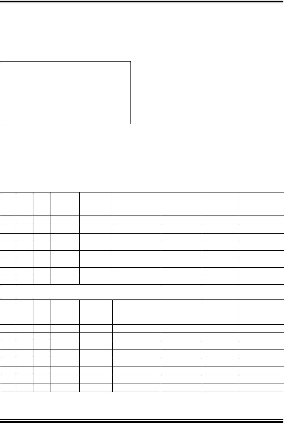
TABLE 4-3: MCP3905L OUTPUT FREQUENCY SETTINGS
F2 F1 F0 HF
C
HF
C
(Hz)
HF
C
(Hz),
MCLK=3.58 MHz
HF
OUT
(Hz),
w/ full scale
AC inputs
F
C
(Hz)
F
C
(Hz),
MCLK=3.58 MHz
00064XF
C
MCLK/2
15
109.25 23.71 MCLK/2
21
1.71
00132XF
C
MCLK/2
15
109.25 23.71 MCLK/2
20
3.41
01016XF
C
MCLK/2
15
109.25 23.71 MCLK/2
19
6.83
0112048XF
C
MCLK/2
7
27968.75 6070.12 MCLK/2
18
13.66
100 8XF
C
MCLK/2
16
54.62 11.85 MCLK/2
19
6.83
10164XF
C
MCLK/2
16
54.62 11.85 MCLK/2
22
0.85
11032XF
C
MCLK/2
16
54.62 11.85 MCLK/2
21
1.71
11116XF
C
MCLK/2
16
54.62 11.85 MCLK/2
20
3.41
TABLE 4-4: MCP3905A/06A OUTPUT FREQUENCY SETTINGS
F2 F1 F0 HF
C
HF
C
(Hz)
HF
C
(Hz),
MCLK=3.58 MHz
HF
OUT
(Hz),
w/ full scale
AC inputs
F
C
(Hz)
F
C
(Hz),
MCLK=3.58 MHz
00064XF
C
MCLK/2
15
109.25 23.71 MCLK/2
21
1.71
00132XF
C
MCLK/2
15
109.25 23.71 MCLK/2
20
3.41
01016XF
C
MCLK/2
15
109.25 23.71 MCLK/2
19
6.83
0112048XF
C
MCLK/2
7
27968.75 6070.12 MCLK/2
18
13.66
100128XF
C
MCLK/2
14
219.51 47.42 MCLK/2
21
1.71
10164XF
C
MCLK/2
14
219.51 47.42 MCLK/2
20
3.41
11032XF
C
MCLK/2
14
219.51 47.42 MCLK/2
19
6.83
11116XF
C
MCLK/2
14
219.51 47.42 MCLK/2
18
13.66