
Datasheet


Table Of Contents
- MCP3905A/05L/06A
- Features
- Description
- Package Type
- Functional Block Diagram
- Notes:
- 1.0 Electrical Characteristics
- 2.0 Typical Performance Curves
- FIGURE 2-1: Measurement Error, Gain = 8 PF = 1.
- FIGURE 2-2: Measurement Error, Gain = 16, PF = 1.
- FIGURE 2-3: Measurement Error, Gain = 32, PF = 1.
- FIGURE 2-4: Measurement Error, Gain = 8, PF = 0.5.
- FIGURE 2-5: Measurement Error, Gain = 16, PF = 0.5.
- FIGURE 2-6: Measurement Error, Gain =32, PF = 0.5.
- FIGURE 2-7: Measurement Error, Gain = 1, PF = 1.
- FIGURE 2-8: Measurement Error, Gain = 2, PF = 1.
- FIGURE 2-9: Measurement Error, Gain = 1, PF = + 0.5.
- FIGURE 2-10: Measurement Error, Gain = 2, PF = + 0.5.
- FIGURE 2-11: Measurement Error, Temperature = +125°C, Gain = 1.
- FIGURE 2-12: Measurement Error, Temperature = +125°C, Gain = 2.
- FIGURE 2-13: Measurement Error, Temperature = +125°C, Gain = 8.
- FIGURE 2-14: Measurement Error, Temperature = +125°C, Gain = 16.
- FIGURE 2-15: Measurement Error vs. Input Frequency.
- FIGURE 2-16: Channel 0 Offset Error (DC Mode, HPF off), G = 1.
- FIGURE 2-17: Channel 0 Offset Error (DC Mode, HPF off), G = 8.
- FIGURE 2-18: Channel 0 Offset Error (DC Mode, HPF Off), G = 16.
- FIGURE 2-19: Measurement Error vs. VDD (G = 16).
- FIGURE 2-20: Measurement Error vs. VDD, G = 16, External VREF.
- FIGURE 2-21: Measurement Error w/ External VREF, (G = 1).
- FIGURE 2-22: Measurement Error w/ External VREF (G = 8).
- FIGURE 2-23: Measurement Error w/ External VREF (G = 16).
- 3.0 Pin Descriptions
- TABLE 3-1: Pin Function Table
- 3.1 Digital VDD (DVDD)
- 3.2 High-Pass Filter Input Logic Pin (HPF)
- 3.3 Analog VDD (AVDD)
- 3.4 Current Channel (CH0-, CH0+)
- 3.5 Voltage Channel (CH1-,CH1+)
- 3.6 Master Clear (MCLR)
- 3.7 Reference (REFIN/OUT)
- 3.8 Analog Ground (AGND)
- 3.9 Frequency Control Logic Pins (F2, F1, F0)
- 3.10 Gain Control Logic Pins (G1, G0)
- 3.11 Oscillator (OSC1, OSC2)
- 3.12 Negative Power Output Logic Pin (NEG)
- 3.13 Ground Connection (DGND)
- 3.14 High-Frequency Output (HFOUT)
- 3.15 Frequency Output (FOUT0, FOUT1)
- 4.0 Device Overview
- 5.0 Applications Information
- 6.0 Packaging Information
- Trademarks
- Worldwide Sales and Service
© 2006-2011 Microchip Technology Inc. DS22011B-page 17
MCP3905A/05L/06A
4.3 Ultra-Low Drift V
REF
The MCP3905A/05L/06A devices contain an internal
voltage reference source specially designed to mini-
mize drift over temperature. This internal V
REF
supplies
reference voltage to both current and voltage channel
ADCs. The typical value of this voltage reference is
2.4V ±100 mV. The internal reference has a very low
typical temperature coefficient of ±15 ppm/°C, allowing
the output frequencies to have minimal variation with
respect to temperature since they are proportional to
(1/V
REF
)².
The output pin for the voltage reference is REFIN/OUT.
Appropriate bypass capacitors must be connected to
the REFIN/OUT pin for proper operation (see
Section 5.0 “Applications Information”). The
voltage reference source impedance is typically 4 kΩ,
which enables this voltage reference to be overdriven
by an external voltage reference source.
If an external voltage reference source is connected to
the REFIN/OUT pin, the external voltage will be used
as the reference for both current and voltage channel
ADCs. The voltage across the source resistor will then
be the difference between the internal and external
voltage. The allowed input range for the external
voltage source goes from 2.2V to 2.6V for accurate
measurement error. A V
REF
value outside of this range
will cause additional heating and power consumption
due to the source resistor, which might affect measure-
ment error.
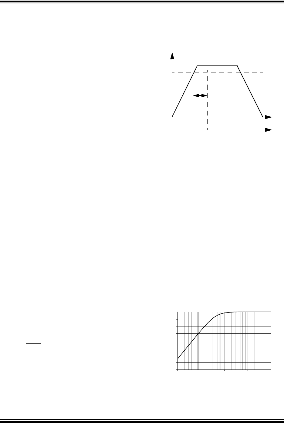
4.4 Power-On Reset (POR)
The MCP3905A/05L/06A devices contain an internal
POR circuit that monitors analog supply voltage AV
DD
during operation. This circuit ensures correct device
startup at system power-up and system power-down
events. The POR circuit has built-in hysteresis and a
timer to give a high degree of immunity to potential
ripple and noise on the power supplies, allowing proper
settling of the power supply during power-up. A 0.1 µF
decoupling capacitor should be mounted as close as
possible to the AV
DD
pin, providing additional transient
immunity (see Section 5.0 “Applications
Information”).
The threshold voltage is typically set at 4V, with a
tolerance of about ±5%. If the supply voltage falls below
this threshold, the MCP3905A/05L/06A devices will be
held in a Reset condition (equivalent to applying logic
‘0’ on the MCLR
pin). The typical hysteresis value is
approximately 200 mV in order to prevent glitches on
the power supply.
Once a power-up event has occurred, an internal timer
prevents the part from outputting any pulse for
approximately 1s (with MCLK = 3.58 MHz), thereby
preventing potential metastability due to intermittent
resets caused by an unsettled regulated power supply.
Figure 4-3 illustrates the different conditions for a
power-up and a power-down event in the typical
conditions.
FIGURE 4-3: Power-on Reset Operation.
4.5 High-Pass Filters and Multiplier
The active real-power value is extracted from the DC
instantaneous power. Therefore, any DC offset
component present on Channel 0 and Channel 1
affects the DC component of the instantaneous power
and will cause the real-power calculation to be
erroneous. In order to remove DC offset components
from the instantaneous power signal, a high-pass filter
has been introduced on each channel. Since the high-
pass filtering introduces phase delay, identical high-
pass filters are implemented on both channels. The
filters are clocked by the same digital signal, ensuring
a phase difference between the two channels of less
than one MCLK period. Under typical conditions
(MCLK = 3.58 MHz), this phase difference is less than
0.005°, with a line frequency of 50 Hz. The cut-off
frequency of the filter (4.45 Hz) has been chosen to
induce minimal gain error at typical line frequencies,
allowing sufficient settling time for the desired
applications. The two high-pass filters can be disabled
by applying logic ‘0’ to the HPF pin.
FIGURE 4-4: HPF Magnitude Response
(MCLK = 3.58 MHz).
AV
DD
5V
4.2V
4V
0V
DEVICE
MODE
RESET
PROPER
OPERATION
RESET
NO
PULSE
OUT
Time
1s
-40
-35
-30
-25
-20
-15
-10
-5
0
0.1 1 10 100 1000
Frequency (Hz)
Normal Mode Rejection (dB)