
Datasheet


Table Of Contents
- MCP3905A/05L/06A
- Features
- Description
- Package Type
- Functional Block Diagram
- Notes:
- 1.0 Electrical Characteristics
- 2.0 Typical Performance Curves
- FIGURE 2-1: Measurement Error, Gain = 8 PF = 1.
- FIGURE 2-2: Measurement Error, Gain = 16, PF = 1.
- FIGURE 2-3: Measurement Error, Gain = 32, PF = 1.
- FIGURE 2-4: Measurement Error, Gain = 8, PF = 0.5.
- FIGURE 2-5: Measurement Error, Gain = 16, PF = 0.5.
- FIGURE 2-6: Measurement Error, Gain =32, PF = 0.5.
- FIGURE 2-7: Measurement Error, Gain = 1, PF = 1.
- FIGURE 2-8: Measurement Error, Gain = 2, PF = 1.
- FIGURE 2-9: Measurement Error, Gain = 1, PF = + 0.5.
- FIGURE 2-10: Measurement Error, Gain = 2, PF = + 0.5.
- FIGURE 2-11: Measurement Error, Temperature = +125°C, Gain = 1.
- FIGURE 2-12: Measurement Error, Temperature = +125°C, Gain = 2.
- FIGURE 2-13: Measurement Error, Temperature = +125°C, Gain = 8.
- FIGURE 2-14: Measurement Error, Temperature = +125°C, Gain = 16.
- FIGURE 2-15: Measurement Error vs. Input Frequency.
- FIGURE 2-16: Channel 0 Offset Error (DC Mode, HPF off), G = 1.
- FIGURE 2-17: Channel 0 Offset Error (DC Mode, HPF off), G = 8.
- FIGURE 2-18: Channel 0 Offset Error (DC Mode, HPF Off), G = 16.
- FIGURE 2-19: Measurement Error vs. VDD (G = 16).
- FIGURE 2-20: Measurement Error vs. VDD, G = 16, External VREF.
- FIGURE 2-21: Measurement Error w/ External VREF, (G = 1).
- FIGURE 2-22: Measurement Error w/ External VREF (G = 8).
- FIGURE 2-23: Measurement Error w/ External VREF (G = 16).
- 3.0 Pin Descriptions
- TABLE 3-1: Pin Function Table
- 3.1 Digital VDD (DVDD)
- 3.2 High-Pass Filter Input Logic Pin (HPF)
- 3.3 Analog VDD (AVDD)
- 3.4 Current Channel (CH0-, CH0+)
- 3.5 Voltage Channel (CH1-,CH1+)
- 3.6 Master Clear (MCLR)
- 3.7 Reference (REFIN/OUT)
- 3.8 Analog Ground (AGND)
- 3.9 Frequency Control Logic Pins (F2, F1, F0)
- 3.10 Gain Control Logic Pins (G1, G0)
- 3.11 Oscillator (OSC1, OSC2)
- 3.12 Negative Power Output Logic Pin (NEG)
- 3.13 Ground Connection (DGND)
- 3.14 High-Frequency Output (HFOUT)
- 3.15 Frequency Output (FOUT0, FOUT1)
- 4.0 Device Overview
- 5.0 Applications Information
- 6.0 Packaging Information
- Trademarks
- Worldwide Sales and Service
© 2006-2011 Microchip Technology Inc. DS22011B-page 15
MCP3905A/05L/06A
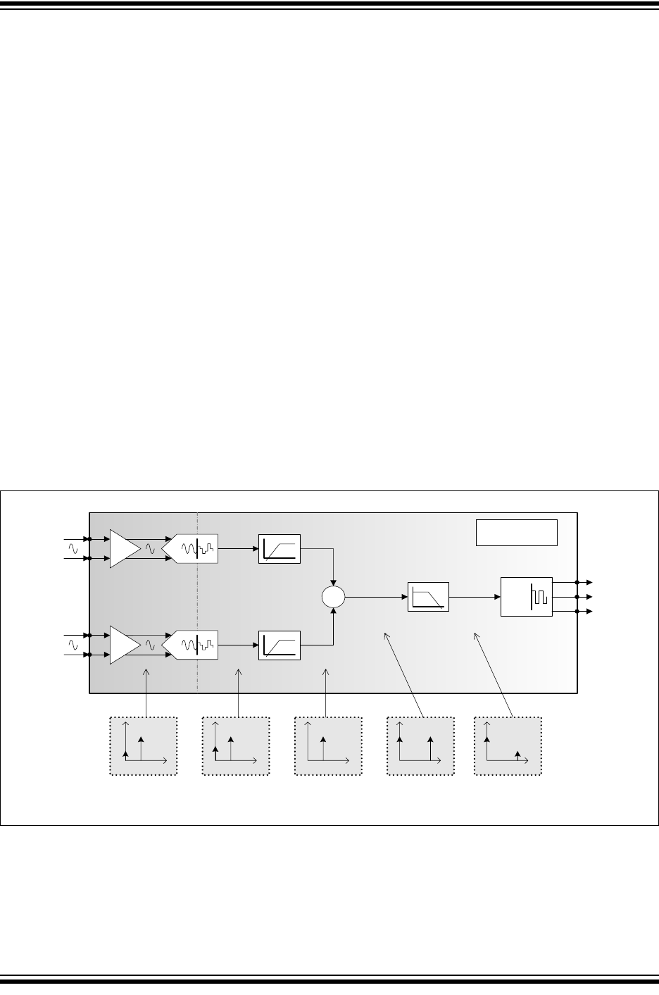
4.0 DEVICE OVERVIEW
The MCP3905A/05L/06A devices are energy metering
ICs that supply a frequency output proportional to
active (real) power, and higher frequency output
proportional to the instantaneous power for meter
calibration. Both channels use 16-bit, second-order,
delta-sigma ADCs that oversample the input at a
frequency equal to MCLK/4, allowing for wide dynamic
range input signals. A Programmable Gain Amplifier
(PGA) increases the usable range on the current input
channel (Channel 0). The calculation of the active
power, and the filtering associated with this calculation
is performed in the digital domain, ensuring better
stability and drift performance. Figure 4-1 represents
the simplified block diagram of the
MCP3905A/05L/06A, detailing its main signal
processing blocks.
Two digital high-pass filters cancel the system offset on
both channels such that the real-power calculation
does not include any circuit or system offset. After
being high-pass filtered, the voltage and current signals
are multiplied to give the instantaneous power signal.
This signal does not contain the DC offset components,
such that the averaging technique can be efficiently
used to give the desired active-power output.
The instantaneous power signal contains the real-
power information; it is the DC component of the
instantaneous power. The averaging technique can be
used with both sinusoidal and non-sinusoidal
waveforms, as well as for all power factors. The
instantaneous power is thus low-pass filtered in order
to produce the instantaneous real-power signal.
A digital-to-frequency converter accumulates the
instantaneous active real power information to produce
output pulses with a frequency proportional to the
average real power. The low-frequency pulses present
at the F
OUT0
and F
OUT1
outputs are designed to drive
electromechanical counters and two-phase stepper
motors displaying the real-power energy consumed.
Each pulse corresponds to a fixed quantity of real
energy, selected by the F2, F1 and F0 logic settings.
The HF
OUT
output has a higher frequency setting and
less integration period such that it can represent the
instantaneous real-power signal. Due to the shorter
accumulation time, it enables the user to proceed to
faster calibration under steady load conditions (see
Section 4.7 “F
OUT0/1
and HF
OUT
Output
Frequencies”).
FIGURE 4-1: Simplified MCP3905A/05L/06A Block Diagram with Frequency Contents.
HPF
...1010..
DTF
–
+
ADC
–
+
PGA
LPF
HPF
X
CH0+
CH0-
CH1+
CH1-
ADC
F
OUT0
F
OUT1
HF
OUT
0 0
MCP3905
Input Signal with
System Offset and
Line Frequency
ADC Output Code
Contains System
and ADC Offset
DC Offset
Removed by HPF
Instantaneous
Power
Instantaneous
Real Power
0 00
Frequency
Content
ANALOG DIGITAL
MCP390X