User manual
Manuals
Brands
MICROCHIP TECHNOLOGY Manuals
Dev Kits
PCB design board
29
30
31
32
33
34
35
36
37
38
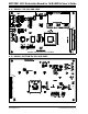
Schema
tics and
Layouts
2010 Microchip Technology Inc.
DS51845B-page 33
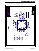
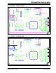
A.10
BOARD – LAYE
R #2 VDD
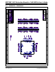
A.1
1
BOARD – LAYE
R #3 GND
1
...
...
31
32
33
34
35
...
...
38